CONTENTS
1.1 Digital Computers and Digital Systems
1.1.1 Applications and types of microprocessors
1.2.2.1 Diminished Radix Complement
1.2.2.3 Subtraction with Complements
1.2.9 Real Numbers - Floating Point
2.2 Converting Analogue Signals
3 Introduction to Digital Signal Processors
3.1 How DSPs are Different from Other Microprocessors
3.2 Characteristics of DSP processors
3.2.3 Input and Output Interfaces
3.2.5 Data formats in DSP processors
3.2.6 Precision and dynamic range
4.1 Features for Reducing Memory Access Requirements
4.4 External Memory Interfaces
4.5 Multiprocessor Support in External Memory Interfaces
5.4 DSP56002 – DSP56156 – DSP96002
5.5 TMS320C25 - TMS320C50 - TMS320C30 - TMS320C40
6 Choosing the Right DSP Processor
6.7 Power Consumption and Management
APPENDIX A - IEEE Standard for Binary Floating Point Arithmetic
APPENDIX B - IEEE Standard for Radix-Independent Floating Point Arithmetic
APPENDIX C – Calculation of Emax and bias
1 Binary Systems
1.1 Digital Computers and Digital Systems
Digital computers have made possible many scientific, industrial, and commercial advances that would have been unattainable otherwise. Our space program would have been impossible without real-time, continuous computer monitoring, and many business enterprises function efficiently only with the aid of automatic data processing. Computers are used in scientific calculations, commercial and business data processing, air traffic control, space guidance, the educational field, and many other areas. The most striking property of a digital computer is its generality; it can follow a sequence of instructions, called a program that operates on given data. The user can specify and change programs and/or data according to the specific need. As a result of this flexibility, general-purpose digital computers can perform a wide variety of information-processing tasks.
The general-purpose digital computer is the best-known example of a digital system. Other examples include telephone switching exchanges, digital voltmeters, digital counters, electronic calculators, and digital displays. Characteristic of a digital system is its manipulation of discrete elements of information. Such discrete elements may be electric impulses, the decimal digits, the letters of an alphabet, arithmetic operations, punctuation marks, or any other set of meaningful symbols. The juxtaposition of discrete elements of information represents a quantity of information. For example, the letters d, o, and g form the word dog. The digits 237 form a number. Thus, a sequence of discrete elements forms a language, that is, a discipline that conveys information. Early digital computers were used mostly for numerical computations. In this case, the discrete elements used are the digits. From this application, the term digital computer has emerged. A more appropriate name for a digital computer would be a “discrete information-processing system.”
Discrete elements of information are represented in a digital system by physical quantities called signals. Electrical signals such as voltages and currents are the most common. The signals in all present-day electronic digital systems have only two discrete values and are said to be binary. The digital-system designer is restricted to the use of binary signals because of the lower reliability of many-valued electronic circuits. In other words, a circuit with ten states, using one discrete voltage value for each state, can be designed, but it would possess a very low reliability of operation. In contrast, a transistor circuit that is either on or off has two possible signal values and can be constructed to be extremely reliable. Because of this physical restriction of components, and because human logic tends to be binary, digital systems that are constrained to take discrete values are further constrained to take binary values.
Discrete quantities of information arise either from the nature of the process or may be quantized from a continuous process. For example, a payroll schedule is an inherently discrete process that contains employee names, social security numbers, weekly salaries, income taxes, etc. An employee’s paycheck is processed using discrete data values such as letters of the alphabet (names), digits (salary), and special symbols such as $. On the other hand, a research scientist may observe continuous process but record only specific quantities in tabular form. The scientist is thus quantizing his continuous data. Each number in his table is a discrete element of information.
Many physical systems can be described mathematically by differential equations whose solutions as a function of time give the complete mathematical behavior of the process. An analog computer performs a direct simulation of a physical system. Each section of the computer is the analog of some particular portion of the process under study. The variables in the analog computer are represented by continuous signals, usually electric voltages that vary with time. The signal variables are considered analogous to those of the process and behave in the same manner. Thus, measurements of the analog voltage can be substituted for variables of the process. The term analog signal is sometimes substituted for continuous signal because “analog computer” has come to mean a computer that manipulates continuous variables.
To simulate a physical process in a digital computer, the quantities must be quantized. When the variables of the process are presented by real-time continuous signals, the latter are quantized by an analog-to-digital conversion device. A physical system whose behavior is described by mathematical equations is simulated in a digital computer by means of numerical methods. When the problem to be processed is inherently discrete, as in commercial applications, the digital computer manipulates the variables in their natural form.
The memory unit of a digital computer stores programs as well as input, output, and intermediate data. The processor unit performs arithmetic and other data-processing tasks as specified by a program. The control unit supervises the flow of information between the various units. The control unit retrieves the instructions, one by one, from the program that is stored in memory. For each instruction, the control unit informs the processor to execute the operation specified by the instruction. Both program and data are stored in memory. The control unit supervises the program instructions, and the processor manipulates the data as specified by the program.
The program and data prepared by the user are transferred into the memory unit by means of an input device such as a keyboard. An output device, such as a printer, receives the result of the computations and the printed results are presented to the user. The input and output devices are special digital systems driven by electromechanical parts and controlled by electronic digital circuits.
An electronic calculator is a digital system similar to a digital computer, with the input device being a keyboard and the output device a numerical display. Instructions are entered in the calculator by means of the function keys, such as plus and minus. Data are entered through the numeric keys. Results are displayed directly in numeric form. Some calculators come close to resembling a digital computer by having printing capabilities and programmable facilities. A digital computer, however, is a more powerful device than a calculator. A digital computer can accommodate many other input and output devices; it can perform not only arithmetic computations, but logical operations as well and can be programmed to make decisions based on internal and external conditions.
It has already been mentioned that a digital computer manipulates discrete elements of information and that these elements are represented in the binary form. Operands used for calculations may be expressed in the binary number system. Other discrete elements, including the decimal digits, are represented in binary codes. Data processing is carried out by means of binary logic elements using binary signals. Quantities are stored in binary storage elements.
1.1.1 Applications and types of microprocessors
Today, microprocessors are found in two major application areas:
• Computer system applications
• Embedded system applications
Embedded systems are often high-volume applications for which manufacturing cost is a key factor. More and more embedded systems are mobile battery-operated systems. For such systems power consumption (battery time) and size are also critical factors. Because they are specifically designed to support a single application, embedded systems only integrate the hardware required to support this application. They often have simpler architectures than computer systems. On the other hand, they often have to perform operations with timings that are much more critical than in computer systems.
A cellular phone for instance must compress the speech in real time; otherwise, the process will produce audible noise. They must also perform with very high reliability. A software crash would be unacceptable in an ABS brake application. Digital Signal Processing applications are often viewed as a third category of microprocessor applications because they use specialized CPUs called DSPs. However, in reality they qualify as specialized embedded applications.
Today, there are 3 different types of microprocessors optimized to be used in each application area:
• Computer systems: General-purpose microprocessors.
• Embedded applications: Microcontrollers
• Signal processing applications: Digital Signal Processors (DSPs)
In reality, the boundaries of application areas are not as well defined as they seem. For instance, DSPs can be used in applications requiring a high computational speed, but not necessarily related to signal processing. Such applications include computer video boards and specialized co-processor boards designed for intensive scientific computation. On the other hand, powerful general-purpose microprocessors are used in high-end digital signal processing equipment designed for algorithm development and rapid prototyping. The following sections list the typical features and application areas for the three types of microprocessors.
General purpose microprocessors
Applications: Computer systems
Manufacturers and models: Intel-Pentium, Motorola-PowerPC, Digital-Alpha Chip, LSI Logic-SPARC family (SUN), ... etc.
Typical features
• Wide address bus allowing the management of large memory spaces
• Integrated hardware memory management unit
• Wide data formats (32 bits or more)
• Integrated co-processor, or Arithmetic Logic Unit supporting complex numerical
operations, such as floating point multiplications.
• Sophisticated addressing modes to efficiently support high-level language functions.
• Large silicon area
• High cost
• High power consumption
Embedded systems: Microcontrollers
Application examples: Television set, wristwatches, TV/VCR remote control, home appliances, musical cards, electronic fuel injection, ABS brakes, hard disk drive, computer mouse / keyboard, USB controller, computer printer, photocopy machine, ... etc.
Manufacturers and models: Motorola-68HC11, Intel-8751, Microchip-PIC16/17family, Cypress-PsoC family, … etc.
Typical features
• Memory and peripherals integrated on the chip
• Narrow address bus allowing only limited amounts of memory.
• Narrow data formats (8 bits or 16 bits typical)
• No coprocessor, limited Arithmetic-Logic Unit.
• Limited addressing modes (High-level language programming is often inefficient)
• Small silicon area
• Low cost
• Low power consumption.
Signal processing: DSPs
Application examples: Telecommunication systems, control systems, altitude, and flight control systems in aerospace applications, audio/video recording, and play-back (compact-disk/MP3 players, video cameras…etc.), high-performance hard-disk drives, modems, video boards, noise cancellation systems, … etc.
Manufacturers and models: Texas Instruments TMS320C6000, TMS320C5000, Motorola 56000, 96000, Analog devices ADSP2100, ADSP21000, ... etc.
Typical features
• Fixed-point processor (TMS320C5000, 56000...) or floating point processor
(TMS320C67, 96000...)
• Architecture optimized for intensive computation. For instance the TMS320C67 can
do 1000 Million floating point operations a second (1 GIGA Flop).
• Narrow address bus supporting a only limited amounts of memory.
• Specialized addressing modes to efficiently support signal processing operations
(circular addressing for filters, bit-reverse addressing for Fast Fourier
Transforms…etc.)
• Narrow data formats (16 bits or 32 bits typical).
• Many specialized peripherals integrated on the chip (serial ports, memory,
timers…etc.)
• Low power consumption.
• Low cost.
1.2 Binary Numbers
A decimal number such as 7392 represents a quantity equal to 7 thousands plus 3 hundreds, plus 9 tens, plus 2 units. The thousands, hundreds, etc. are powers of 10 implied by the position of the coefficients. To be more exact, 7392 should be written as
7 ´ 103 + 3 ´ 102 + 9 ´ 101 + 2 ´ 100
However, the convention is to write only the coefficients and from their position deduce the necessary powers of 10. In general, a number with a decimal point is represented by a series of coefficients as follows:
a5 a4 a3 a2 al a0 . a-1 a-2 a-3
The aj coefficients are one of the ten digits (0, 1, 2, … , 9), and the subscript value j gives the place value and, hence, the power of 10 by which the coefficient must be multiplied.
105a5 + 104a4 + 103a3 + l02a2 + l01a1 + l00a0 + 10-1a-1 + 10-2a-2 + 10-3a-3
The decimal number system is said to be of base, or radix, 10 because it uses ten digits and the coefficients are multiplied by powers of 10. In the binary system, the coefficients of the binary numbers system have two possible values: 0 and 1. Each coefficient a, is multiplied by 2’. For example, the decimal equivalent of the binary number 11010.11 is 26.75, as shown from the multiplication of the coefficients by powers of 2:
1 ´ 24 + 1 ´ 23 + 0 ´ 22 + 1 ´ 21 + 0 ´ 20 + 1 ´ 2-1 + 1 ´ 2-2 = 26.75
In general, a number expressed in base-r system has coefficients multiplied by powers of r:
an . rn + an-1 . rn-1 + … + a2 . r2 + a1 . r + a0 + a-1 . r-1 + a-2 . r-2 + … + a-m . r-m
The coefficients aj range in value from 0 to r-1. To distinguish between numbers of different bases, we enclose the coefficients in parentheses and write a subscript equal to the base used (except sometimes for decimal numbers, where the content makes it obvious that it is decimal).
1.2.1 Arithmetic Operations
Arithmetic operations with numbers in base r follow the same rules as for decimal numbers. When other than the familiar base 10 is used, one must be careful to use only the r allowable digits. Examples of addition, subtraction, and multiplication of two binary numbers are as follows:
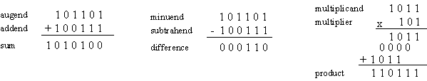
Figure 1‑1: Binary arithmetic operations.
The sum of two binary numbers is calculated by the same rules as in decimal, except that the digits of the sum in any significant position can be only 0 or 1. Any carry obtained in a given significant position is used by the pair of digits one significant position higher. The subtraction is slightly more complicated. The rules are still the same as in decimal, except that the borrow in a given significant position adds 2 to a minuend digit. (A borrow in the decimal system adds 10 to a minuend digit.) Multiplication is very simple. The multiplier digits are always 1 or 0. Therefore, the partial products are equal either to the multiplicand or to 0.
1.2.2 Complements
Complements are used in digital computers for simplifying the subtraction operation and for logical manipulation. There are two types of complements for each base-r system: the radix complement and the diminished radix complement. The first is referred to as the r’s complement and the second as the (r-1)‘s complement. When the value of the base r is substituted in the name, the two types are referred to as the 2’s complement and 1’s complement for binary numbers, and the 10’s complement and 9’s complement for decimal numbers.
1.2.2.1 Diminished Radix Complement
Given a number N in base r having n digits, the (r-l)’s complement of N is defined as:
![]()
For decimal numbers, r = 10 and r-1 = 9, so the 9’s complement of N is (10n-1)-N. Now, 10n represents a number that consists of a single 1 followed by n 0’s. 10n-1 is a number represented by n 9’s. For example, if n = 4, we have l04 = 10,000 and l04-1 = 9999. It follows that the 9’s complement of a decimal number is obtained by subtracting each digit from 9. Some numerical examples follow.
The 9’s complement of 546700 is 999999 - 546700 = 453299.
The 9’s complement of 012398 is 999999 – 012398 = 987601.
For binary numbers, r = 2 and r-1 = 1, so the l’s complement of N is (2n-1)-N. Again. 2n is represented by a binary number that consists of a 1 followed by n 0’s. 2 n-1 is a binary number represented by n 1‘s. For example, if n = 4, we have 2 4 = (10000)2 and 24-1 = (1111)2. Thus, the l’s complement of a binary number is obtained by subtracting each digit from 1. However, when subtracting binary digits from 1. we can have either 1-0 = 1 or 1-1=0, which causes the bit to change from 0 to 1 or from 1 to 0. Therefore, the l’s complement of a binary number is formed by changing l’s to 0’s and 0’s to l’s. The following are some numerical examples.
The l’s complement of 1011000 is 0100111.
The l’s complement of 0101101 is 1010010.
1.2.2.2 Radix Complement
The r’s complement of an n-digit number N in base r is defined as rn-N for N ¹ 0 and 0 for N=0. Comparing with the (r-1)’s complement, we note that the r’ s complement is obtained by adding 1 to the (r-1)’s complement since rn-N = [(rn-1)-N ] + 1. Thus, the 10’s complement of decimal 2389 is 7610 + 1=7611 and is obtained by adding 1 to the 9’s-complement value. The 2’s complement of binary 101100 is 010011 + 1 = 010100 and is obtained by adding 1 to the 1’s-complement value.
Since 10n is a number represented by a 1 followed by n 0’s, l0n-N, which is the 10’s complement of N, can be formed also by leaving all least significant 0’s unchanged, subtracting the first nonzero least significant digit from 10, and subtracting all higher significant digits from 9.
The 10’s complement of 012398 is 987602.
The 10’s complement of 246700 is 753300.
The 10’s complement of the first number is obtained by subtracting 8 from 10 in the least significant position and subtracting all other digits from 9. The 10’s complement of the second number is obtained by leaving the two least significant 0’s unchanged, subtracting 7 from 10. and subtracting the other three digits from 9.
Similarly, the 2’s complement can be formed by leaving all least significant 0’s and the first 1 unchanged, and replacing l’s with 0’s and 0’s with l’s in all other higher significant digits.
The 2’s complement of 1101100 is 0010100.
The 2’s complement of 0110111 is 1001001.
The 2’s complement of the first number is obtained by leaving the two least significant 0’s and the first 1 unchanged, and then replacing l’s with 0’s and 0’s with l’s in the other four most-significant digits. The 2’s complement of the second number is obtained by leaving the least significant 1 unchanged and complementing all other digits.
In the previous definitions, it was assumed that the numbers do not have a radix point. If the original number N contains a radix point, the point should be removed temporarily in order to form the r’s or (r-l)’s complement. The radix point is then restored to the complemented number in the same relative position. It is also worth mentioning that the complement of the complement restores the number to its original value. The r’s complement of N is rn-N. The complement of the complement is r-(rn-N)=N, giving back the original number.
1.2.2.3 Subtraction with Complements
The direct method of subtraction taught in elementary schools uses the borrow concept. In this method, we borrow a 1 from a higher significant position when the minuend digit is smaller than the subtrahend digit. This seems to be easiest when people perform subtraction with paper and pencil. When subtraction is implemented with digital hardware, this method is found to be less efficient than the method that uses complements.
The subtraction of two n-digit unsigned numbers M-N in base r can be done as follows:
1. Add the minuend M to the r’s complement of the subtrahend N. This performs M + (rn- N) = M - N + rn.
2. If M ³ N, the sum will produce an end carry, rn, which is discarded; what is left is the result M-N.
3. If M < N, the sum does not produce an end carry and is equal to rn-(N – M), which is the r’s complement of (N - M). To obtain the answer in a familiar form, take the r’s complement of the sum and place a negative sign in front.
The following examples illustrate the procedure.
Example: Using 10’s complement, subtract 72532 - 3250.

Note that M has 5 digits and N has only 4 digits. Both numbers must have the same number of digits; so we can write N as 03250. Taking the 10’s complement of N produces a 9 in the most significant position. The occurrence of the end carry signifies that M - N and the result is positive.
Example: Using 10’s complement, subtract 3250 – 72532.

Note that since 3250 < 72532, the result is negative. Since we are dealing with unsigned numbers, there is really no way to get an unsigned result for this case. When subtracting with complements, the negative answer is recognized from the absence of the end carry and the complemented result. When working with paper and pencil, we can change the answer to a signed negative number in order to put it in a familiar form. Subtraction with complements is done with binary numbers in a similar manner using the same procedure outlined before.
1.2.3 Signed Binary Numbers
Positive integers including zero can be represented as unsigned numbers. However, to represent negative integers, we need a notation for negative values. In ordinary arithmetic, a negative number is indicated by a minus sign and a positive number by a plus sign. Because of hardware limitations, computers must represent everything with binary digits, commonly referred to as bits. It is customary to represent the sign with a bit placed in the leftmost position of the number. The convention is to make the sign bit 0 for positive and 1 for negative.
It is important to realize that both signed and unsigned binary numbers consist of a string of bits when represented in a computer. The user determines whether the number is signed or unsigned. If the binary number is signed, then the leftmost bit represents the sign and the rest of the hits represent the number. If the binary number is assumed to be unsigned, then the leftmost bit is the most significant bit of the number. For example, the string of bits 01001 can be considered as 9 (unsigned binary) or a +9 (signed binary) because the leftmost bit is 0. The string of bits 11001 represent the binary equivalent of 25 when considered as an unsigned number or as -9 when considered as a signed number because of the 1 in the leftmost position, which designates negative, and the other four bits, which represent binary 9. Usually, there is no confusion in identifying the bits if the type of representation for the number is known in advance.
The representation of the signed numbers in the last example is referred to as the signed-magnitude convention. In this notation, the number consists of a magnitude and a symbol (+ or -) or a bit (0 or 1) indicating the sign. This is the representation of signed numbers used in ordinary arithmetic. When arithmetic operations are implemented in a computer, it is more convenient to use a different system for representing negative numbers, referred to as the signed-complement system. In this system, a negative number is indicated by its complement. Whereas the signed-magnitude system negates a number by changing its sign, the signed-complement system negates a number by taking its complement. Since positive numbers always start with 0 (plus) in the leftmost position, the complement will always start with a 1, indicating a negative number. The signed-complement system can use either the 1’s or the 2’s complement, but the 2’s complement is the most common.
As an example, consider the number 9 represented in binary with eight bits. +9 is represented with a sign bit of 0 in the leftmost position followed by the binary equivalent of 9 to give 00001001. Note that all eight bits must have a value and, therefore, 0’s are inserted following the sign bit up to the first 1. Although there is only one way to represent +9, there are three different ways to represent -9 with eight bits:
In
signed-magnitude
representation
: 10001001
In signed-1’s-complement
representation
: 11110110
In signed-2’s-complement representation
: 11110111
In signed-magnitude, -9 is obtained from +9 by changing the sign bit in the leftmost position from 0 to 1. In signed-1’s complement, -9 is obtained by complementing all the bits of +9, including the sign bit. The signed-2’s-complement representation of –9 is obtained by taking the 2’s complement of the positive number, including the sign bit.
The signed-magnitude system is used in ordinary arithmetic, but is awkward when employed in computer arithmetic. Therefore, the signed-complement is normally used. The l’s complement imposes some difficulties and is seldom used for arithmetic operations except in some older computers. The 1’s complement is useful as a logical operation since the change of 1 to 0 or 0 to I is equivalent to a logical complement operation, as will be shown in the next chapter. The following discussion of signed binary arithmetic deals exclusively with the signed-2’s-complement representation of negative numbers. The same procedures can be applied to the signed-i ‘s-complement system by including the end-around carry as done with unsigned numbers.
1.2.4 Arithmetic Addition
The addition of two numbers in the signed-magnitude system follows the rules of ordinary arithmetic. If the signs are the same, we add the two magnitudes and give the sum the common sign. If the signs are different, we subtract the smaller magnitude from the larger and give the result the sign of the larger magnitude. For example, (+25) + (-37)=-(37-25) = -12 and is done by subtracting the smaller magnitude 25 from the larger magnitude 37 and using the sign of 37 for the sign of the result. This is a process that requires the comparison of the signs and the magnitudes and then performing either addition or subtraction. The same procedure applies to binary numbers in signed-magnitude representation. In contrast, the rule for adding numbers in the signed-complement system does not require a comparison or subtraction, but only addition. The procedure is very simple and can be stated as follows for binary numbers.
The addition of two signed binary numbers with negative numbers represented in signed-2’s-complement form is obtained from the addition of the two numbers, including their sign bits. A carry out of the sign-bit position is discarded. Numerical examples for addition follow. Note that negative numbers must be initially in 2’s complement and that the sum obtained after the addition if negative is in 2’s-complement form.


In each of the four cases, the operation performed is addition with the sign bit included. Any carry out of the sign-bit position is discarded, and negative results are automatically in 2’s-complement form.
In order to obtain a correct answer, we must ensure that the result has a sufficient number of bits to accommodate the sum. If we start with two n-bit numbers and the sum occupies n+1 bits, we say that an overflow occurs. When one performs the addition with paper and pencil, an overflow is not a problem since we are not limited by the width of the page. We just add another 0 to a positive number and another 1 to a negative number in the most-significant position to extend them to n + 1 bits and then perform the addition. Overflow is a problem in computers because the number of bits that hold a number is finite, and a result that exceeds the finite value by 1 cannot be accommodated.
The complement form of representing negative numbers is unfamiliar to those used to the signed-magnitude system. To determine the value of a negative number when in signed-2’s complement. it is necessary to convert it to a positive number to place it in a more familiar form. For example, the signed binary number 11111001 is negative because the leftmost bit is 1. Its 2’s complement is 00000111, which is the binary equivalent of +7. We therefore recognize the original negative number to be equal to -7.
1.2.5 Arithmetic Subtraction
Subtraction of two signed binary numbers when negative numbers are in 2’s-complement form is very simple and can be stated as follows: Take the 2’s complement of the subtrahend (including the sign bit) and add-it to the minuend (including the sign bit). A carry out of the sign-bit position is discarded. This procedure occurs because a subtraction operation can be changed to an addition operation if the sign of the subtrahend is changed. This is demonstrated by the following relationship:
(± A)-(+ B) = (± A) + (-B)
(± A)-(- B) = (± A) + (+B)
But changing a positive number to a negative number is easily done by taking its 2’s complement. The reverse is also true because the complement of a negative number in complement form produces the equivalent positive number. Consider the subtraction of (-6) - (-13) = + 7. In binary with eight bits, this is written as (11111010-11110011). The subtraction is changed to addition by taking the 2’s complement of the subtrahend (-13) to give (+13). In binary, this is 11111010 + 00001101 = 100000111. Removing the end carry, we obtain the correct answer 00000111 (+7).
It is worth noting that binary numbers in the signed-complement system are added and subtracted by the same basic addition and subtraction rules as unsigned numbers. Therefore, computers need only one common hardware circuit to handle both types of arithmetic. The user or programmer must interpret the results of such addition or subtraction differently, depending on whether it is assumed that the numbers are signed or unsigned.
1.2.6 Binary Multiplication
Binary multiplication is carried out in very much the same manner as decimal multiplication, obtaining partial products in the conventional manner, but adding the latter in binary fashion. That is, write down the multiplier and the multiplicand, multiply entire multiplicand by each multiplier digit in turn, and add the partial results. In binary multiplication, 0 × 0 = 0, 0 × 1 = 0, 1 × 0 = 0, and 1 × 1 = 1. Example, multiply 10111 (binary 23) by 11001 (binary 25):

Since computers cannot handle blanks, trailing zeros should be filled in where necessary. Note that, every digit in a binary number is either 1 or 0, so every step in multiplication requires either adding or not adding. This process requires the ability to add, and shift left. In a left shift, digits migrate left, most significant bit is lost, least significant bit is set to 0. Multiplication is a repeated addition. Regarding to the multiplication of negative numbers, since addition of negative twos complement numbers works, so multiplication works too.


1.2.7 Binary Division
Binary division is carried out in a manner similar to decimal division, operates symmetrically to multiplication, the difference being that one subtracts instead of adds and shifts right to divide by 2 instead of multiplying by 2, , as the following example will show: Divide 1001 (binary 9) by 0100 (binary 4)


If we assume a fixed length register of and 2’s complement number representation and the divisor and dividend are both assumed to be positive integers, after initialization, first step will be the normalization operation which is: shift the divisor to the left until the leftmost 1 is just to the right of the sign bit while counting the number of shifts. For example:
01101101 dividend (109)
00010101 divisor (21)
00101010 first shift
01010100 second shift
The next step will subtraction and shifting loop. Note that if the subtraction is positive, the quotient has a 1 in the current bit position. The quotient string is built incrementally by adding the result for the current but position to the end of the quotient, and shifting left.
1.2.8 Fixed Point (Integers)
Fixed-point representation is used to store integers, the positive and negative whole numbers. In the simplest case, the 216=65,536 possible bit patterns are assigned to the numbers 0 through 65,535. This is called unsigned integer format, and a simplified example is shown in Figure 1‑2 (using only 4 bits per number). Conversion between the bit pattern and the number being represented is nothing more than changing between base 2 (binary) and base 10 (decimal). The disadvantage of unsigned integer is that negative numbers cannot be represented.
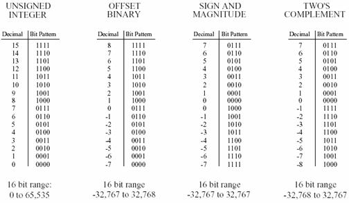
Figure 1‑2: Fixed point binary representations.
Offset binary is similar to unsigned integer, except the decimal values are shifted to allow for negative numbers. In the 4 bit example of Figure 1‑2, the decimal numbers are offset by seven, resulting in the 16 bit patterns corresponding to the integer numbers -7 through 8. In this same manner, a 16 bit representation would use 32,767 as an offset, resulting in a range between -32,767 and 32,768. Offset binary is not a standardized format, and you will find other offsets used, such 32,768. The most important use of offset binary is in ADC and DAC. For example, the input voltage range of -5v to 5v might be mapped to the digital numbers 0 to 4095, for a 12 bit conversion.
Sign and magnitude is another simple way of representing negative integers. The far left bit is called the sign bit, and is made a zero for positive numbers, and a one for negative numbers. The other bits are a standard binary representation of the absolute value of the number. This results in one wasted bit pattern, since there are two representations for zero, 0000 (positive zero) and 1000 (negative zero). This encoding scheme results in 16 bit numbers having a range of -32,767 to 32,767.
These first three representations are conceptually simple, but difficult to implement in hardware. Remember, when A=B+C is entered into a computer program, some hardware engineer had to figure out how to make the bit pattern representing B, combine with the bit pattern representing C, to form the bit pattern representing A. Two's complement is the format loved by hardware engineers, and is how integers are usually represented in computers. To understand the encoding pattern, look first at decimal number zero in Figure 1‑2, which corresponds to a binary zero, 0000. As we count upward, the decimal number is simply the binary equivalent (0 = 0000, 1 = 0001, 2 = 0010, 3 = 0011, etc.). If we again start at 0000 and begin subtracting, the digital hardware automatically counts in two's complement: 0 = 0000, -1 = 1111, -2 = 1110, -3 = 1101, etc. This is analogous to the odometer in a new automobile. If driven forward, it changes: 00000, 00001, 00002, 00003, and so on. When driven backwards, the odometer changes: 00000, 99999, 99998, 99997, etc.
Using 16 bits, two's complement can represent numbers from -32,768 to 32,767. The left most bit is a 0 if the number is positive or zero, and a 1 if the number is negative. Consequently, the left most bit is called the sign bit, just as in sign and magnitude representation. Converting between decimal and two's complement is straightforward for positive numbers, a simple decimal to binary conversion. For negative numbers, the following algorithm is often used: take the absolute value of the decimal number, convert it to binary, and complement all of the bits (ones become zeros and zeros become ones), add 1 to the binary number. Two's complement is hard for humans, but easy for digital electronics.
1.2.9 Real Numbers - Floating Point
The usual method used by computers to represent real numbers is floating point notation. The encoding scheme for floating point numbers is more complicated than for fixed point. There are many varieties of floating point notation and each has individual characteristics. The key concept is that, a real number is represented by a number called a mantissa, times a base raised to an integer power, called an exponent. The base is usually fixed, and the mantissa and exponent vary to represent different real numbers. For example, the number 387.53 could be represented as 38753×10-2. The mantissa is 38753, and the exponent is –2. Other possible representations are 0.38753×10³ and 387.53×100. We choose the representation in which the mantissa is an integer with no trailing 0s.
Floating point representation is similar to scientific notation, except everything is carried out in base two, rather than base ten. While several similar formats are in use, the most common is ANSI/IEEE Std. 754-1985. This standard defines the format for 32 bit numbers called single precision, as well as 64 bit numbers called double precision. As shown in Figure 1‑3, the 32 bits used in single precision are divided into three separate groups: bits 0 through 22 form the mantissa, bits 23 through 30 form the exponent, and bit 31 is the sign bit.
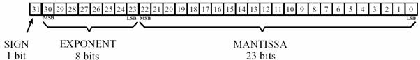
Figure 1‑3: Single precision floating point bit pattern.
These bits form the floating-point number, v, by the following relation:
![]()
where S is the value of the sign bit, M is the value of the mantissa, and E is the value of the mantissa. The term (-1)S, simply means that the sign bit, S, is 0 for a positive number and 1 for a negative number. The variable, E, is the number between 0 and 255 represented by the eight exponent bits. Subtracting 127 from this number allows the exponent term to run from 2-127 to 2128. In other words, exponent is stored in offset binary with an offset of 127. The mantissa, M, is formed from the 23 bits as a binary fraction. For example, the decimal fraction: 2.783, is interpreted: 2 + 7/10 + 8/100 + 3/1000. The binary fraction: 1.0101 means: 1 + 0/2 + 1/4 + 0/8 + 1/16. Floating point numbers are normalized in the same way as scientific notation, that is, there is only one nonzero digit left of the decimal point (called a binary point in base 2). Since the only nonzero number that exists in base two is 1, the leading digit in the mantissa will always be a 1, and therefore does not need to be stored. Removing this redundancy allows the number to have an additional one bit of precision. The 23 stored bits, referred to by the notation: m22 m21 m20 … m0, form the mantissa according to:
![]()
In other words, M = 1 + m222-1 + m212-2+ m202-3…. If bits 0 through 22 are all zeros, M takes on the value of one. If bits 0 through 22 are all ones, M is just a hair under two, i.e., 2-2-23.
Using this encoding scheme, the largest number that can be represented is: ±(2-2-23)×2128 = ± 6.8 × 1038. Likewise, the smallest number that can be represented is: ± 1.0 × 2-127 = ± 5.9 × 10-39. The IEEE standard reduces this range slightly to free bit patterns that are assigned special meanings. In particular, the largest and smallest numbers allowed in the standard are ± 3.4 × 1038 and ± 1.2 × 10-38 respectively. The freed bit patterns allow three, special classes of numbers: ±0 is defined as all of the mantissa and exponent bits being zero. ± 4 is defined as all of the mantissa bits being zero, and all of the exponent bits being one. A group of very small unnormalized numbers between ±1.2×10-38 and ±1.4 × 10-45. These are lower precision numbers obtained by removing the requirement that the leading digit in the mantissa be a one. Besides these three special classes, there are bit patterns that are not assigned a meaning, commonly referred to as NANs (Not A Number).
The IEEE standard for double precision simply adds more bits to both the mantissa and exponent. Of the 64 bits used to store a double precision number, bits 0 through 51 are the mantissa, bits 52 through 62 are the exponent, and bit 63 is the sign bit. As before, the mantissa is between one and just under two. The 11 exponent bits form a number between 0 and 2047, with an offset of 1023, allowing exponents from 2-1023 to 21024. The largest and smallest numbers allowed are ±1.8×10308 and ±2.2×10-308 respectively. These are incredibly large and small numbers! It is quite uncommon to find an application where single precision is not adequate. You will probably never find a case where double precision limits what you want to accomplish.
1.2.10 Number Precision
The errors associated with number representation are very similar to quantization errors during ADC. You want to store a continuous range of values; however, you can represent only a finite number of quantized levels. Every time a new number is generated, after a math calculation for example, it must be rounded to the nearest value that can be stored in the format you are using.
As an example, imagine that you allocate 32 bits to store a number. Since there are exactly different bit patterns possible, you can 232 = 4,294,967,296 represent exactly 4,294,967,296 different numbers. Some programming languages allow a variable called a long integer, stored as 32 bits, fixed point, two's complement. This means that the 4,294,967,296 possible bit patterns represent the integers between -2,147,483,648 and 2,147,483,647. In comparison, single precision floating point spreads these 4,294,967,296 bit patterns over the much larger range: -3.4 × 1038 to 3.4 × 1038.
With fixed-point variables, the gaps between adjacent numbers are always exactly one. In floating point notation, the gaps between adjacent numbers vary over the represented number range. If we randomly pick a floating point number, the gap next to that number is approximately ten million times smaller than the number itself (to be exact, 2-24 to 2-23 times the number). This is a key concept of floating point notation: large numbers have large gaps between them, while small numbers have small gaps. Figure 1‑4 illustrates this by showing consecutive floating-point numbers, and the gaps that separate them.
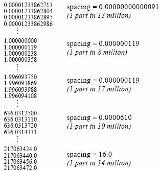
Figure 1‑4: The gaps between adjacent numbers.
2 DSP Review
2.1 Basics
Digital Signal Processing (DSP) is used in a wide variety of applications, and it is hard to find a good definition that is general. We can start by dictionary definitions of the words. Digital is operating by the use of discrete signals to represent data in the form of numbers. Signal is a variable parameter by which information is conveyed through an electronic circuit. Processing is to perform operations on data according to programmed instructions. This leads us to a simple definition: Digital Signal processing is changing or analyzing information which is measured as discrete sequences of numbers. Note two unique features of Digital Signal processing as opposed to plain old ordinary digital processing: signals come from the real world - this intimate connection with the real world leads to many unique needs such as the need to react in real time and a need to measure signals and convert them to digital numbers, and signals are discrete - which means the information in between discrete samples is lost.
The advantages of DSP are common to many digital systems and include versatility, repeatability, and simplicity. Versatility: digital systems can be reprogrammed for other applications (at least where programmable DSP chips are used) and digital systems can be ported to different hardware (for example a different DSP chip or board level product). Repeatability: digital systems can be easily duplicated, digital systems do not depend on strict component tolerances, and digital system responses do not drift with temperature. Simplicity: some things can be done more easily digitally than with analogue systems.
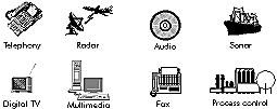
Figure 2‑1: Applications of Digital Signal Processing.
DSP is used in a very wide variety of applications (Figure 2‑1) but most share some common features: they use a lot of maths (multiplying and adding signals), they deal with signals that come from the real world, and they require a response in a certain time. Where general purpose DSP processors are concerned, most applications deal with signal frequencies that are in the audio range.
2.2 Converting Analogue Signals
Most DSP applications deal with analogue signals where the analogue signal has to be converted to digital form as shown in Figure 2‑2. The analogue signal - a continuous variable defined with infinite precision - is converted to a discrete sequence of measured values which are represented digitally. Information is lost in converting from analogue to digital, due to: inaccuracies in the measurement, uncertainty in timing, and the limits on the duration of the measurement. These effects are called quantization errors.
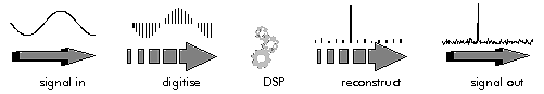
Figure 2‑2: The analog to digital process of DSP.
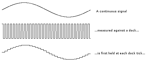
Figure 2‑3: Digitization of an analog signal.
The continuous analogue signal has to be held before it can be sampled. Otherwise, the signal would be changing during the measurement. Only after it has been held can the signal be measured, and the measurement converted to a digital value (Figure 2‑3).

Figure 2‑4: Sampled signal.
The sampling results in a discrete set of digital numbers that represent measurements of the signal - usually taken at equal intervals of time (Figure 2‑4). Note that the sampling takes place after the hold. This means that we can sometimes use a slower Analogue to Digital Converter (ADC) than might seem required at first sight. The hold circuit must act fast enough that the signal is not changing during the time the circuit is acquiring the signal value, but the ADC has all the time that the signal is held to make its conversion. We don't know what we don't measure. In the process of measuring the signal, some information is lost (Figure 2‑5). Sometimes we may have some a priori knowledge of the signal, or be able to make some assumptions that will let us reconstruct the lost information.
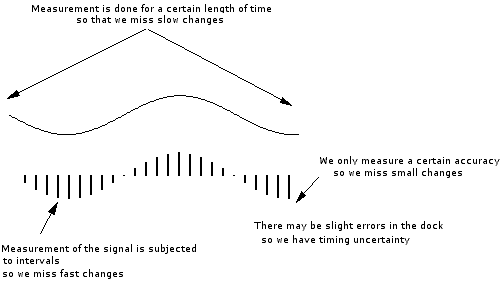
Figure 2‑5: The loss of information during sampling.
2.3 Aliasing
We only sample the signal at intervals that we don't know what happened between the samples. A crude example is to consider a 'glitch' that happened to fall between adjacent samples. Since we don't measure it, we have no way of knowing the glitch was there at all.
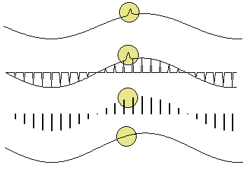
Figure 2‑6: The aliasing artifact. Loss of information.
In a less obvious case, we might have signal components that are varying rapidly in between samples. Again, we could not track these rapid inter-sample variations (Figure 2‑6). Therefore, we must sample fast enough to see the most rapid changes in the signal. Sometimes we may have some a priori knowledge of the signal, or be able to make some assumptions about how the signal behaves in between samples. If we do not sample fast enough, we cannot track completely the most rapid changes in the signal.
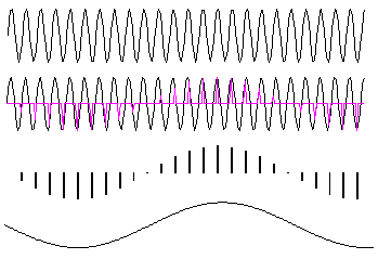
Figure 2‑7: Sampling at slow rates.
Some higher frequencies can be incorrectly interpreted as lower ones. In Figure 2‑7, the high frequency signal is sampled just under twice every cycle. The result is that each sample is taken at a slightly later part of the cycle. If we draw a smooth connecting line between the samples, the resulting curve looks like a lower frequency. This is called 'aliasing' because one frequency looks like another.
Note that the problem of aliasing is that we cannot tell which frequency we have - a high frequency looks like a low one so we cannot tell the two apart. But sometimes we may have some a priori knowledge of the signal, or be able to make some assumptions about how the signal behaves in between samples, that will allow us to tell unambiguously what we have.
Nyquist showed that to distinguish unambiguously between all signal frequency components we must sample faster than twice the frequency of the highest frequency component.
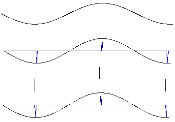
Figure 2‑8: Sampling high frequency signal. A continuous signal sampled twice per cycle has enough information to be reconstructed.
In Figure 2‑8, the high frequency signal is sampled twice every cycle. If we draw a smooth connecting line between the samples, the resulting curve looks like the original signal. But if the samples happened to fall at the zero crossings, we would see no signal at all - this is why the sampling theorem demands we sample faster than twice the highest signal frequency. This avoids aliasing. The highest signal frequency allowed for a given sample rate is called the Nyquist frequency. Actually, Nyquist says that we have to sample faster than the signal bandwidth, not the highest frequency. But this leads us into multirate signal processing which is a more advanced subject.
2.4 Antialiasing
Nyquist showed that to distinguish unambiguously between all signal frequency components we must sample at least twice the frequency of the highest frequency component. To avoid aliasing, we simply filter out all the high frequency components before sampling (Figure 2‑9).
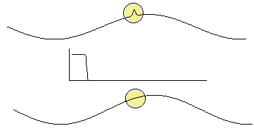
Figure 2‑9: The effect of antialiasing filter. High frequency components are removed through a low pass filter.
Note that antialias filters must be analogue - it is too late once you have done the sampling. This simple brute force method avoids the problem of aliasing. But it does remove information - if the signal had high frequency components, we cannot now know anything about them.
Although Nyquist showed that provide we sample at least twice the highest signal frequency we have all the information needed to reconstruct the signal, the sampling theorem does not say the samples will look like the signal.
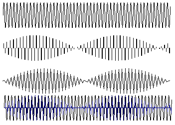
Figure 2‑10: A high frequency signal sampled fast enough may still look wrong but can be reconstructed.
Figure 2‑10 shows a high frequency sine wave that is nevertheless sampled fast enough according to Nyquist's sampling theorem - just more than twice per cycle. When straight lines are drawn between the samples, the signal's frequency is indeed evident - but it looks as though the signal is amplitude modulated. This effect arises because each sample is taken at a slightly earlier part of the cycle. Unlike aliasing, the effect does not change the apparent signal frequency. The answer lies in the fact that the sampling theorem says there is enough information to reconstruct the signal - and the correct reconstruction is not just to draw straight lines between samples.
The signal is properly reconstructed from the samples by low pass filtering: the low pass filter should be the same as the original antialias filter. The reconstruction filter interpolates between the samples to make a smoothly varying analogue signal. In Figure 2‑11, the reconstruction filter interpolates between samples in a 'peaky' way that seems at first sight to be strange. The explanation lies in the shape of the reconstruction filter's impulse response.
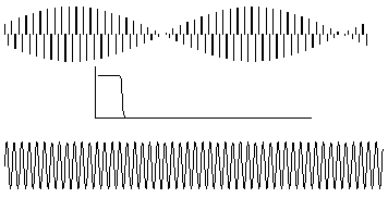
Figure 2‑11: A sampled signal must be low-pass filtered to reconstruct the original.
The impulse response of the reconstruction filter has a classic 'sin(x)/x shape. The stimulus fed to this filter is the series of discrete impulses which are the samples. Every time an impulse hits the filter, we get 'ringing' - and it is the superposition of all these peaky rings that reconstructs the proper signal. If the signal contains frequency components that are close to the Nyquist, then the reconstruction filter has to be very sharp indeed. This means it will have a very long impulse response - and so the long 'memory' needed to fill in the signal even in region of the low amplitude samples.
2.5 Frequency resolution
Sampling of the signal is done only for a certain time. We cannot see slow changes in the signal if we don't wait long enough. In fact we must sample for long enough to detect not only low frequencies in the signal, but also small differences between frequencies. The length of time for which we are prepared to sample the signal determines our ability to resolve adjacent frequencies - the frequency resolution.
We must sample for at least one complete cycle of the lowest frequency we want to resolve. We can see that we face a forced compromise. We must sample fast to avoid and for a long time to achieve a good frequency resolution. But sampling fast for a long time means we will have a lot of samples - and lots of samples means lots of computation, for which we generally don't have time. So we will have to compromise between resolving frequency components of the signal, and being able to see high frequencies.
2.6 Quantization
When the signal is converted to digital form, the precision is limited by the number of bits available. Figure 2‑12 shows an analogue signal which is then converted to a digital representation - in this case, with 8 bit precision. The smoothly varying analogue signal can only be represented as a 'stepped' waveform due to the limited precision. Sadly, the errors introduced by digitization are both non linear and signal dependent. Non linear means we cannot calculate their effects using normal math. Signal dependent means the errors are coherent and so cannot be reduced by simple means.
This is a common problem in DSP. The errors due to limited precision (i.e. word length) are non linear (hence incalculable) and signal dependent (hence coherent). Both are bad news, and mean that we cannot really calculate how a DSP algorithm will perform in limited precision - the only reliable way is to implement it, and test it against signals of the type expected. The non linearity can also lead to instability - particularly with IIR filters. The word length of hardware used for DSP processing determines the available precision and dynamic range.
Figure 2‑12: Limited precision leads to errors which are signal dependent.
Figure 2‑13: Timing error leads to value error, an accurate dock leads to accurate values. An error in the dock translates the error in the values.
Uncertainty in the clock timing leads to errors in the sampled signal. Figure 2‑13 shows an analogue signal which is held on the rising edge of a clock signal. If the clock edge occurs at a different time than expected, the signal will be held at the wrong value. Sadly, the errors introduced by timing error are both non linear and signal dependent.
A real DSP system suffers from three sources of error due to limited word length in the measurement and processing of the signal: limited precision due to word length when the analogue signal is converted to digital form, errors in arithmetic due to limited precision within the processor itself, and limited precision due to word length when the digital samples are converted back to analogue form.
These errors are often called quantization error. The effects of quantization error are in fact both non linear and signal dependent. Non linear means we cannot calculate their effects using normal math. Signal dependent means that even if we could calculate their effect, we would have to do so separately for every type of signal we expect. A simple way to get an idea of the effects of limited word length is to model each of the sources of quantization error as if it were a source of random noise.
The model of quantization as injections of random noise is helpful in gaining an idea of the effects. But it is not actually accurate, especially for systems with feedback like IIR filters. The effect of quantization error is often similar to an injection of random noise.
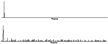
Figure 2‑14: Quantization error. The spectrum of a pure tone is noisy when quantized.
Figure 2‑14 shows the spectrum calculated from a pure tone. The top plot shows the spectrum with high precision (double precision floating point) and the bottom plot shows the spectrum when the sine wave is quantized to 16 bits. The effect looks very like low level random noise. The signal to noise ratio is affected by the number of bits in the data format, and by whether the data is fixed point or floating point.
2.7 Summary
A DSP system has three fundamental sources of limitation:
- loss of information because we only take samples of the signal at intervals
- loss of information because we only sample the signal for a certain length of time
- errors due to limited precision (i.e. word length) in data storage and arithmetic
The effects of these limitations are as follows:
- aliasing is the result of sampling, which means we cannot distinguish between high and low frequencies
- limited frequency resolution is the result of limited duration of sampling, which means we cannot distinguish between adjacent frequencies
- quantization error is the result of limited precision (word length) when converting between analogue and digital forms, when storing data, or when performing arithmetic
Aliasing and frequency resolution are fundamental limitations - they arise from the mathematics and cannot be overcome. They are limitations of any sampled data system, not just digital ones.
Quantization error is an artifact of the imperfect precision, and can be improved upon by using an increased word length. It is a feature peculiar to digital systems. Its effects are non linear and signal dependent, but can sometimes be acceptably modeled as injections of random noise.
3 Introduction to Digital Signal Processors
3.1 How DSPs are Different from Other Microprocessors
The last forty years have shown that computers are extremely capable in two broad areas, data manipulation, such as word processing and database management, and mathematical calculation, used in science, engineering, and Digital Signal Processing. All microprocessors can perform both tasks; however, it is difficult (expensive) to make a device that is optimized for both. There are technical tradeoffs in the hardware design, such as the size of the instruction set and how interrupts are handled. Even more important, there are marketing issues involved: development and manufacturing cost, competitive position, product lifetime, and so on. As a broad generalization, these factors have made traditional microprocessors, such as the Pentium, primarily directed at data manipulation. Similarly, DSPs are designed to perform the mathematical calculations needed in Digital Signal Processing.
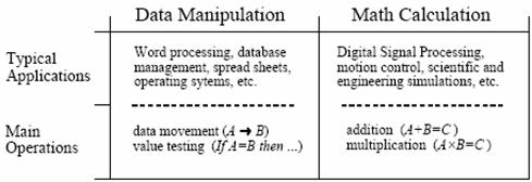
Figure 3‑1: Data manipulation versus mathematical calculation.
Figure 3‑1 lists the most important differences between these two categories. Data manipulation involves storing and sorting information. For instance, consider a word processing program. The basic task is to store the information (typed in by the operator), organize the information (cut and paste, spell checking, page layout, etc.), and then retrieve the information (such as saving the document on a floppy disk or printing it with a laser printer). These tasks are accomplished by moving data from one location to another, and testing for inequalities (A=B, A<B, etc.). As an example, imagine sorting a list of words into alphabetical order. Each word is represented by an 8 bit number, the ASCII value of the first letter in the word. Alphabetizing involved rearranging the order of the words until the ASCII values continually increase from the beginning to the end of the list. This can be accomplished by repeating two steps over-and-over until the alphabetization is complete. First, test two adjacent entries for being in alphabetical order (IF A>B THEN ...). Second, if the two entries are not in alphabetical order, switch them so that they are (A«B). When this two-step process is repeated many times on all adjacent pairs, the list will eventually become alphabetized.
As another example, consider how a document is printed from a word processor. The computer continually tests the input device (mouse or keyboard) for the binary code that indicates, "print the document." When this code is detected, the program moves the data from the computer's memory to the printer. Here we have the same two basic operations: moving data and inequality testing. While mathematics is occasionally used in this type of application, it is infrequent and does not significantly affect the overall execution speed.
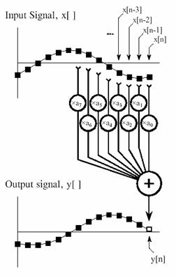
Figure 3‑2: FIR digital filter. Each sample in the output signal is found by multiplying samples from the input signal by the kernel coefficients and summing the products.
In comparison, the execution speed of most DSP algorithms is limited almost completely by the number of multiplications and additions required. For example, Figure 3‑2 shows the implementation of an FIR digital filter, the most common DSP technique. Using the standard notation, the input signal is referred to by x[ ], while the output signal is denoted by y[ ]. Our task is to calculate the sample at location n in the output signal. An FIR filter performs this calculation by multiplying appropriate samples from the input signal by a group of coefficients, denoted by a0, a1, a2, a3,…, and then adding the products. This is simply saying that the input signal has been convolved with a filter kernel consisting of a0, a1, a2, a3,…. Depending on a0, a1, a2, a3... the application, there may only be a few coefficients in the filter kernel, or many thousands. While there is some data transfer and inequality evaluation in this algorithm, such as to keep track of the intermediate results and control the loops, the math operations dominate the execution time.
In addition to performing mathematical calculations very rapidly, DSPs must also have a predictable execution time. Suppose you launch your desktop computer on some task, say, converting a word-processing document from one form to another. It does not matter if the processing takes ten milliseconds or ten seconds; you simply wait for the action to be completed before you give the computer its next assignment.
In comparison, most DSPs are used in applications where the processing is continuous, not having a defined start or end. For instance, consider an engineer designing a DSP system for an audio signal, such as a hearing aid. If the digital signal is being received at 20,000 samples per second, the DSP must be able to maintain a sustained throughput of 20,000 samples per second. However, there are important reasons not to make it any faster than necessary. As the speed increases, so does the cost, the power consumption, the design difficulty, and so on. This makes an accurate knowledge of the execution time critical for selecting the proper device, as well as the algorithms that can be applied.
3.2 Characteristics of DSP processors
Although there are many DSP processors, they are mostly designed with the same few basic operations in mind, that they share the same set of basic characteristics. These characteristics fall into three categories:
- SSpecialized high speed arithmetic
- DData transfer to and from the real world
- MMultiple access memory architectures
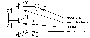
Figure 3‑3: Typical DSP operations require specific functions.
Typical DSP operations require a few specific operations. Figure 3‑3 shows an FIR filter and illustrates the basic DSP operations: additions and multiplications, delays, and array handling. Each of these operations has its own special set of requirements. Additions and multiplications require us to fetch two operands, perform the addition or multiplication (usually both), store the result, or hold it for a repetition. Delays require us to hold a value for later use. Array handling requires us to fetch values from consecutive memory locations, and copy data from memory to memory. To suit these fundamental operations DSP processors often have parallel multiply and add, multiple memory accesses (to fetch two operands and store the result), lots of registers to hold data temporarily, efficient address generation for array handling, and special features such as delays or circular addressing.
3.2.1 Circular Buffering
Digital Signal Processors are designed to quickly carry out FIR filters and similar techniques. To understand the hardware, we must first understand the algorithms. To start, we need to distinguish between off-line processing and real-time processing. In off-line processing, the entire input signal resides in the computer at the same time. For example, a geophysicist might use a seismometer to record the ground movement during an earthquake. After the shaking is over, the information may be read into a computer and analyzed in some way. Another example of off-line processing is medical imaging, such as CT and MRI. The data set is acquired while the patient is inside the machine, but the image reconstruction may be delayed until a later time. The key point is that all of the information is simultaneously available to the processing program. This is common in scientific research and engineering, but not in consumer products. Off-line processing is the realm of personal computers and mainframes.
(a) (b)
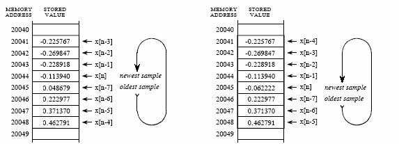
Figure 3‑4: Circular buffer operation. a. Circular buffer at some instant and b. Circular buffer after next sample.
In real-time processing, the output signal is produced at the same time that the input signal is being acquired. For example, this is needed in telephone communication, hearing aids, and radar. These applications must have the information immediately available, although it can be delayed by a short amount. For instance, a 10-millisecond delay in a telephone call cannot be detected by the speaker or listener. Likewise, it makes no difference if a radar signal is delayed by a few seconds before being displayed to the operator. Real-time applications input a sample, perform the algorithm, and output a sample, over-and-over. Alternatively, they may input a group of samples, perform the algorithm, and output a group of samples. This is the world of Digital Signal Processors.
Now imagine that the FIR filter in Figure 3‑2 being implemented in real-time. To calculate the output sample, we must have access to a certain number of the most recent samples from the input. For example, suppose we use eight coefficients in this filter. This means we must know the value of the eight most recent samples from the input signal. These eight samples must be stored in memory and continually updated as new samples are acquired. What is the best way to manage these stored samples? The answer is circular buffering. Figure 3‑4 illustrates an eight sample circular buffer. We have placed this circular buffer in eight consecutive memory locations, 20041 to 20048. Figure 3‑4 (a) shows how the eight samples from the input might be stored at one particular instant in time, while (b) shows the changes after the next sample is acquired. The idea of circular buffering is that the end of this linear array is connected to its beginning; memory location 20041 is viewed as being next to 20048, just as 20044 is next to 20045. You keep track of the array by a pointer that indicates where the most recent sample resides. For instance, in (a) the pointer contains the address 20044, while in (b) it contains 20045. When a new sample is acquired, it replaces the oldest sample in the array, and the pointer is moved one address ahead. Circular buffers are efficient because only one value needs to be changed when a new sample is acquired.
3.2.2 Mathematics
To perform the simple arithmetic required, DSP processors need special high-speed arithmetic units. Most DSP operations require additions and multiplications together. So DSP processors usually have hardware adders and multipliers which can be used in parallel within a single instruction. Figure 3‑5 shows the data path for the Lucent DSP32C processor. The hardware multiply and add work in parallel so that in the space of a single instruction, both an add and a multiply can be completed.
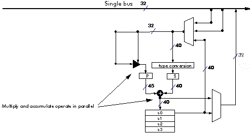
Figure 3‑5: The data path for the Lucent DSP32C processor.
Delays require that intermediate values be held for later use. This may also be a requirement, for example, when keeping a running total - the total can be kept within the processor to avoid wasting repeated reads from and writes to memory. For this reason DSP processors have lots of registers which can be used to hold intermediate values. Registers may be fixed point or floating point format.
Array handling requires that data can be fetched efficiently from consecutive memory locations. This involves generating the next required memory address. For this reason DSP processors have address registers which are used to hold addresses and can be used to generate the next needed address efficiently:
The ability to generate new addresses efficiently is a characteristic feature of DSP processors. Usually, the next needed address can be generated during the data fetch or store operation, and with no overhead. DSP processors have rich sets of address generation operations.
|
*rP |
register indirect |
Read the data pointed to by the address in register rP |
|
*rP++ |
post increment |
Having read the data, post increment the address pointer to point to the next value in the array |
|
*rP-- |
post decrement |
Having read the data, post decrement the address pointer to point to the previous value in the array |
|
*rP++rI |
register post increment |
Having read the data, post increment the address pointer by the amount held in register rI to point to rI values further down the array |
|
*rP++rIr |
bit reversed |
Having read the data, post increment the address pointer to point to the next value in the array, as if the address bits were in bit reversed order |
Figure 3‑6: Addressing modes for the Lucent DSP32C processor.
Figure 3‑6 shows some addressing modes for the Lucent DSP32C processor. The assembler syntax is very similar to C language. Whenever an operand is fetched from memory using register indirect addressing, the address register can be incremented to point to the next needed value in the array. This address increment is free - there is no overhead involved in the address calculation - and in the case of the Lucent DSP32C, processor up to three such addresses may be generated in each single instruction. Address generation is an important factor in the speed of DSP processors at their specialized operations.
The last addressing mode - bit reversed - shows how specialized DSP processors can be. Bit reversed addressing arises when a table of values has to be reordered by reversing the order of the address bits:
- reverse the order of the bits in each address
- shuffle the data so that the new, bit reversed, addresses are in ascending order
This operation is required in the Fast Fourier Transform - and just about nowhere else. So one can see that DSP processors are designed specifically to calculate the Fast Fourier Transform efficiently.
3.2.3 Input and Output Interfaces
In addition to the mathematics, in practice DSP is mostly dealing with the real world. Although this aspect is often forgotten, it is of great importance and marks some of the greatest distinctions between DSP processors and general-purpose microprocessors.
In a typical DSP application, the processor will have to deal with multiple sources of data from the real world (Figure 3‑7). In each case, the processor may have to be able to receive and transmit data in real time, without interrupting its internal mathematical operations. There are three sources of data from the real world:
- Signals coming in and going out
- Communication with an overall system controller of a different type
- Communication with other DSP processors of the same type
These multiple communications routes mark the most important distinctions between DSP processors and general-purpose processors. The need to deal with these different sources of data efficiently leads to special communication features on DSP processors:
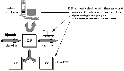
Figure 3‑7: Communication of DSP with overall system controllers.
When DSP processors first came out, they were rather fast processors: for example the first floating point DSP - the AT&T DSP32 - ran at 16 MHz at a time when PC computer clocks were 5 MHz. This meant that we had very fast floating point processors: a fashionable demonstration at the time was to plug a DSP board into a PC and run a fractal (Mandelbrot) calculation on the DSP and on a PC side by side. The DSP fractal was of course faster. Today, however, the fastest DSP processor is the Texas TMS320C6201, which runs at 200 MHz. This is no longer very fast compared with an entry level PC. In addition, the same fractal today will actually run faster on the PC than on the DSP. However, DSP processors are still used - why? The answer lies only partly in that the DSP can run several operations in parallel: a far more basic answer is that the DSP can handle signals very much better than a Pentium. Try feeding eight channels of high quality audio data in and out of a Pentium simultaneously in real time, without affecting the processor performance, if you want to see a real difference.
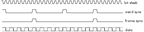
Figure 3‑8: The four activities on a synchronous serial port.
Signals tend to be fairly continuous, but at audio rates or not much higher. They are usually handled by high-speed synchronous serial ports. Serial ports are inexpensive - having only two or three wires - and are well suited to audio or telecommunications data rates up to 10 Mbit/s. Most modern speech and audio analogue to digital converters interface to DSP serial ports with no intervening logic. A synchronous serial port requires only three wires: clock, data, and word sync (Figure 3‑8). The addition of a fourth wire (frame sync) and a high impedance state when not transmitting makes the port capable of Time Division Multiplex (TDM) data handling, which is ideal for telecommunications:
DSP processors usually have synchronous serial ports - transmitting clock and data separately - although some, such as the Motorola DSP56000 family, have asynchronous serial ports as well (where the clock is recovered from the data). Timing is versatile, with options to generate the serial clock from the DSP chip clock or from an external source. The serial ports may also be able to support separate clocks for receive and transmit - a useful feature, for example, in satellite modems where the clocks are affected by Doppler shifts. Most DSP processors also support companding to A-law or mu-law in serial port hardware with no overhead - the Analog Devices ADSP2181 and the Motorola DSP56000 family does this in the serial port, whereas the Lucent DSP32C has a hardware compander in its data path instead.
The serial port will usually operate under DMA - data presented at the port is automatically written into DSP memory without stopping the DSP - with or without interrupts. It is usually possible to receive and transmit data simultaneously.
The serial port has dedicated instructions which make it simple to handle. Because it is standard to the chip, this means that many types of actual I/O hardware can be supported with little or no change to code - the DSP program simply deals with the serial port, no matter to what I/O hardware this is attached.
Host communications is an element of many, though not all, DSP systems. Many systems will have another, general purpose, processor to supervise the DSP: for example, the DSP might be on a PC plug-in card or a VME card - simpler systems might have a microcontroller to perform a 'watchdog' function or to initialize the DSP on power up. Whereas signals tend to be continuous, host communication tends to require data transfer in batches - for instance to download a new program or to update filter coefficients. Some DSP processors have dedicated host ports which are designed to communicate with another processor of a different type, or with a standard bus. For instance the Lucent DSP32C has a host port which is effectively an 8 bit or 16 bit ISA bus: the Motorola DSP56301 and the Analog Devices ADSP21060 have host ports which implement the PCI bus.
The host port will usually operate under DMA - data presented at the port is automatically written into DSP memory without stopping the DSP - with or without interrupts. It is usually possible to receive and transmit data simultaneously.
The host port has dedicated instructions, which make it simple to handle. The host port imposes a welcome element of standardization to plug-in DSP boards - because it is standard to the chip, it is relatively difficult for individual designers to make the bus interface different. For example, of the 22 main different manufacturers of PC plug-in cards using the Lucent DSP32C, 21 are supported by the same PC interface code: this means it is possible to swap between different cards for different purposes, or to change to a cheaper manufacturer, without changing the PC side of the code. Of course this is not foolproof - some engineers will always 'improve upon' a standard by making something incompatible if they can - but at least it limits unwanted creativity.
Interprocessor communications is needed when a DSP application is too much for a single processor - or where many processors are needed to handle multiple but connected data streams. Link ports provide a simple means to connect several DSP processors of the same type. The Texas TMS320C40 and the Analog Devices ADSP21060 both have six link ports (called 'comm. ports' for the 'C40). These would ideally be parallel ports at the word length of the processor, but this would use up too many pins (six ports each 32 bits wide=192, which is a lot of pins even if we neglect grounds). So a hybrid called serial/parallel is used: in the 'C40, comm. ports are 8 bits wide and it takes four transfers to move one 32 bit word - in the 21060, link ports are 4 bits wide and it takes 8 transfers to move one 32 bit word.
The link port will usually operate under DMA - data presented at the port is automatically written into DSP memory without stopping the DSP - with or without interrupts. It is usually possible to receive and transmit data simultaneously. This is a lot of data movement - for example the Texas TMS320C40 could in principle use all its six comm. ports at their full rate of 20 MByte/s to achieve data transfer rates of 120 MByte/s. In practice, of course, such rates exist only in the dreams of marketing men since other factors such as internal bus bandwidth come into play.
The link ports have dedicated instructions which make them simple to handle. Although they are sometimes used for signal I/O, this is not always a good idea since it involves very high speed signals over many pins and it can be hard for external hardware to exactly meet the timing requirements.
3.2.4 Architecture of the DSP
One of the biggest bottlenecks in executing DSP algorithms is transferring information to and from memory. This includes data, such as samples from the input signal and the filter coefficients, as well as program instructions, the binary codes that go into the program sequencer. For example, suppose we need to multiply two numbers that reside somewhere in memory. To do this, we must fetch three binary values from memory, the numbers to be multiplied, plus the program instruction describing what to do. To fetch the two operands in a single instruction cycle, we need to be able to make two memory accesses simultaneously. Actually, since we also need to store the result - and to read the instruction itself - we really need more than two memory accesses per instruction cycle.
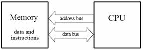
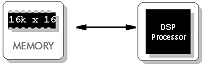
Figure 3‑9: The Von Neumann architecture uses a single memory to hold both data and instructions.
Figure 3‑9 shows how this seemingly simple task is done in a traditional microprocessor. This is often called Von Neumann architecture. Von Neumann architecture contains a single memory and a single bus for transferring data into and out of the central processing unit (CPU). Multiplying two numbers requires at least three clock cycles, one to transfer each of the three numbers over the bus from the memory to the CPU. We don't count the time to transfer the result back to memory, because we assume that it remains in the CPU for additional manipulation (such as the sum of products in an FIR filter). Since the von Neumann architecture uses only a single memory bus, it is cheap, requiring less pins, and simple to use because the programmer can place instructions or data anywhere throughout the available memory. But it does not permit multiple memory accesses.
The modified von Neumann architecture allows multiple memory accesses per instruction cycle by the simple trick of running the memory clock faster than the instruction cycle. For example the Lucent DSP32C runs with an 80 MHz clock: this is divided by four to give 20 million instructions per second (MIPS), but the memory clock runs at the full 80 MHz - each instruction cycle is divided into four 'machine states' and a memory access can be made in each machine state, permitting a total of four memory accesses per instruction cycle (Figure 3‑10). In this case the modified von Neumann architecture permits all the memory accesses needed to support addition or multiplication: fetch of the instruction; fetch of the two operands; and storage of the result.
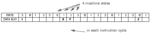
Figure 3‑10: Multiple memory accesses per instruction cycle in modified von Neumann architecture. Four memory accesses per instruction cycle.
The Von Neumann design is quite satisfactory when you are content to execute all of the required tasks in serial. In fact, most computers today are of the Von Neumann design. We only need other architectures when very fast processing is required, and we are willing to pay the price of increased complexity. This leads us to the Harvard architecture, shown Figure 3‑11. This is named for the work done at Harvard University in the 1940s under the leadership of Howard Aiken (1900-1973). As shown in this illustration, Aiken insisted on separate memories for data and program instructions, with separate buses for each. Since the buses operate independently, program instructions and data can be fetched at the same time, improving the speed over the single bus design. Most present day DSPs use this dual bus architecture.
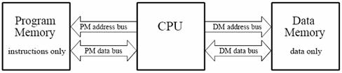
Figure 3‑11: The Harvard architecture uses separate memories for data and instructions, providing higher speed.
The Harvard architecture has two separate physical memory buses. This allows two simultaneous memory accesses. The true Harvard architecture dedicates one bus for fetching instructions, with the other available to fetch operands. This is inadequate for DSP operations, which usually involve at least two operands. So DSP Harvard architectures usually permit the program bus to be used also for access of operands. Note that it is often necessary to fetch three things - the instruction plus two operands - and the Harvard architecture is inadequate to support this.
The Harvard architecture requires two memory buses. This makes it expensive to bring off the chip - for example a DSP using 32 bit words and with a 32 bit address space requires at least 64 pins for each memory bus - a total of 128 pins if the Harvard architecture is brought off the chip. This results in very large chips, which are difficult to design into a circuit.
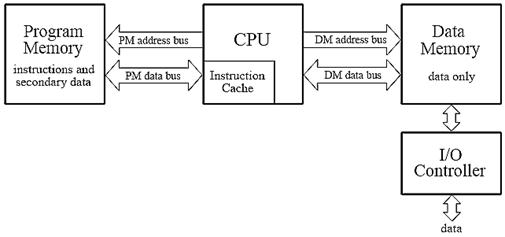
Figure 3‑12: The Super Harvard Architecture improves upon the Harvard design by adding an instruction cache and a dedicated I/O controller.
Figure 3‑12 illustrates the next level of sophistication, the Super Harvard Architecture. This term was coined by Analog Devices to describe the The Scientist and Engineer's Guide to Digital Signal Processing 510 internal operation of their ADSP-2106x and new ADSP-211xx families of Digital Signal Processors. These are called SHARC® DSPs, a contraction of the longer term, Super Harvard Architecture. The idea is to build upon the Harvard architecture by adding features to improve the throughput. While the SHARC DSPs are optimized in dozens of ways, two areas are important enough to be included in Figure 3‑12: an instruction cache, and an I/O controller. First, let's look at how the instruction cache improves the performance of the Harvard architecture. A handicap of the basic Harvard design is that the data memory bus is busier than the program memory bus. When two numbers are multiplied, two binary values (the numbers) must be passed over the data memory bus, while only one binary value (the program instruction) is passed over the program memory bus. To improve upon this situation, we start by relocating part of the "data" to program memory. For instance, we might place the filter coefficients in program memory, while keeping the input signal in data memory. (This relocated data is called "secondary data" in the illustration).
At first glance, this doesn't seem to help the situation; now we must transfer one value over the data memory bus (the input signal sample), but two values over the program memory bus (the program instruction and the coefficient). In fact, if we were executing random instructions, this situation would be no better at all.
However, DSP algorithms generally spend most of their execution time in loops. This means that the same set of program instructions will continually pass from program memory to the CPU. The Super Harvard architecture takes advantage of this situation by including an instruction cache in the CPU. This is a small memory that contains about 32 of the most recent program instructions. The first time through a loop, the program instructions must be passed over the program memory bus. This results in slower operation because of the conflict with the coefficients that must also be fetched along this path. However, on additional executions of the loop, the program instructions can be pulled from the instruction cache. This means that all of the memory to CPU information transfers can be accomplished in a single cycle: the sample from the input signal comes over the data memory bus, the coefficient comes over the program memory bus, and the program instruction comes from the instruction cache. In the jargon of the field, this efficient transfer of data is called a high memory access bandwidth.
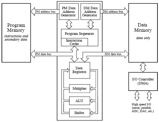
Figure 3‑13: Typical DSP architecture. Digital Signal Processors are designed to implement tasks in parallel. This simplified diagram is the Analog Devices SHARC DSP.
Figure 3‑13 presents a more detailed view of the SHARC architecture, showing the I/O controller connected to data memory. This is how the signals enter and exit the system. For instance, the SHARC DSPs provides both serial and parallel communications ports. These are extremely high speed connections. For example, at a 40 MHz clock speed, there are two serial ports that operate at 40 MBits/second each, while six parallel ports each provide a 40 Mbytes/second data transfer. When all six parallel ports are used together, the data transfer rate is an incredible 240 Mbytes/second.
Both Harvard and von Neuman architectures require the programmer to be careful of where in memory data is placed: for example with the Harvard architecture, if both needed operands are in the same memory bank then they cannot be accessed simultaneously.
3.2.5 Data formats in DSP processors
DSP processors store data in fixed or floating point formats. It is worth noting that fixed point format is not quite the same as integer (Figure 3‑14). The integer format is straightforward: representing whole numbers from 0 up to the largest whole number that can be represented with the available number of bits. Fixed point format is used to represent numbers that lie between 0 and 1, with a binary point assumed to lie just after the most significant bit. The most significant bit in both cases carries the sign of the number. The size of the fraction represented by the smallest bit is the precision of the fixed point format. The size of the largest number that can be represented in the available word length is the dynamic range of the fixed point format.
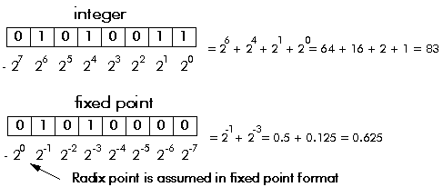
Figure 3‑14: The comparison integer and fixed point data formats.
To make the best use of the full available word length in the fixed point format, the programmer has to make some decisions. If a fixed point number becomes too large for the available word length, the programmer has to scale the number down, by shifting it to the right: in the process lower bits may drop off the end and be lost. If a fixed point number is small, the number of bits actually used to represent it is small. The programmer may decide to scale the number up, in order to use more of the available word length. In both cases the programmer has to keep a track of by how much the binary point has been shifted, in order to restore all numbers to the same scale at some later stage.
Floating point format has the remarkable property of automatically scaling all numbers by moving, and keeping track of, the binary point so that all numbers use the full word length available but never overflow.
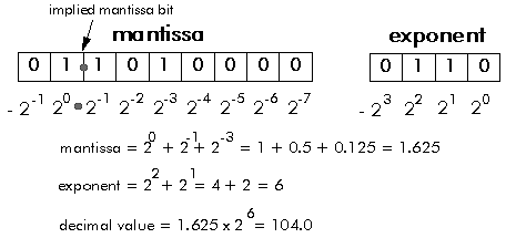
Figure 3‑15: The floating point format.
Floating point numbers have two parts: the mantissa, which is similar to the fixed point part of the number, and an exponent which is used to keep track of how the binary point is shifted (Figure 3‑15). Every number is scaled by the floating point hardware. If a number becomes too large for the available word length, the hardware automatically scales it down, by shifting it to the right. If a number is small, the hardware automatically scales it up, in order to use the full available word length of the mantissa. In both cases the exponent is used to count how many times the number has been shifted. In floating point numbers the binary point comes after the second most significant bit in the mantissa.
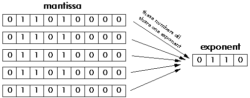
Figure 3‑16: The block floating point format.
The block floating point format in Figure 3‑16 provides some of the benefits of floating point, but by scaling blocks of numbers rather than each individual number. Block floating point numbers are actually represented by the full word length of a fixed point format. If any one of a block of numbers becomes too large for the available word length, the programmer scales down all the numbers in the block, by shifting them to the right. If the largest of a block of numbers is small, the programmer scales up all numbers in the block, in order to use the full available word length of the mantissa. In both cases the exponent is used to count how many times the numbers in the block have been shifted.
Some specialized processors, such as those from Zilog, have special features to support the use of block floating point format. More usually, it is up to the programmer to test each block of numbers and carry out the necessary scaling.
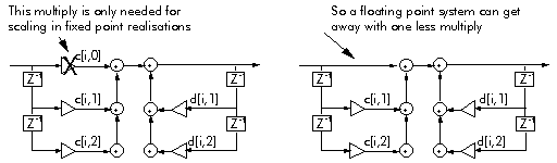
Figure 3‑17: The advantage of floating point format over fixed point. Floating point hardware automatically scales every number to avoid overflow.
The floating point format has one further advantage over fixed point: it is faster. Because of quantization error, a basic direct form 1 IIR filter second order section requires an extra multiplier, to scale numbers and avoid overflow. But the floating point hardware automatically scales every number to avoid overflow, so this extra multiplier is not required (Figure 3‑17).
3.2.6 Precision and dynamic range
The precision with which numbers can be represented is determined by the word length in the fixed point format, and by the number of bits in the mantissa in the floating point format. In a 32 bit DSP processor the mantissa is usually 24 bits, so the precision of a floating point DSP is the same as that of a 24 bit fixed point processor. But floating point has one further advantage over fixed point: because the hardware automatically scales each number to use the full word length of the mantissa, the full precision is maintained even for small numbers (Figure 3‑18).
There is a potential disadvantage to the way floating point works. Because the hardware automatically scales and normalizes every number, the errors due to truncation and rounding depend on the size of the number. If we regard these errors as a source of quantization noise, then the noise floor is modulated by the size of the signal. Although the modulation can be shown to be always downwards (that is, a 32 bit floating point format always has noise which is less than that of a 24 bit fixed point format), the signal dependent modulation of the noise may be undesirable, notably, the audio industry prefers to use 24 bit fixed point DSP processors over floating point because it is thought by some that the floating point noise floor modulation is audible. The precision directly affects quantization error.
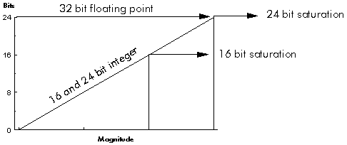
Figure 3‑18: The floating point hardware automatically scales each number and the full precision is maintained even for small numbers
The largest number which can be represented determines the dynamic range of the data format. In fixed point format this is straightforward: the dynamic range is the range of numbers that can be represented in the available word length. For floating point format, though, the binary point is moved automatically to accommodate larger numbers, so the dynamic range is determined by the size of the exponent. Therefore the dynamic range of a floating point format is enormously larger than for a fixed point format (Figure 3‑19).
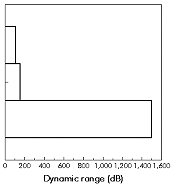
Figure 3‑19: The dynamic range comparison of floating point format over fixed point.
While the dynamic range of a 32 bit floating point format is large, it is not infinite, thus it is possible to suffer overflow and underflow even with a 32 bit floating point format. A classic example of this can be seen by running fractal (Mandelbrot) calculations on a 32 bit DSP processor. After quite a long time, the fractal pattern ceases to change because the increment size has become too small for a 32 bit floating point format to represent.
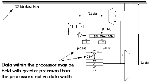
Figure 3‑20: The data path of the Lucent DSP32C
Most DSP processors have extended precision registers within the processor. Figure 3‑20 shows the data path of the Lucent DSP32C processor. Although this is a 32 bit floating point processor, it uses 40 and 45 bit registers internally, thus, results can be held to a wider dynamic range internally than when written to memory.
4 Memory Architectures
DSP processor data paths are optimized to provide extremely high performance on certain kinds of arithmetic-intensive algorithms. However, a powerful data path is, at best, only part of a high-performance processor. To keep the data path fed with data and to store the results of data path operations, DSP processors require the ability to move large amounts of data to and from memory quickly.
DSP processor data paths are designed to perform a multiply-accumulate operation in one instruction cycle. This means that the arithmetic operations required for one tap can be computed in one instruction cycle. However, to achieve this performance, the processor must be able to make several accesses to memory within one instruction cycle. Specifically, the processor must:
- fetch the multiply-accumulate instruction,
- read the appropriate data value from the delay line,
- read the appropriate coefficient value, and
- write the data value to the next location in the delay line to shift data through the delay line.
Thus, the processor must make four accesses to memory in one instruction cycle if the multiply-accumulate operation is to execute in a single instruction cycle. In practice, some processors use other techniques (as discussed later) to reduce the actual number of memory accesses needed to three or even two. Nevertheless, all processors require multiple memory accesses within one instruction cycle. This level of memory bandwidth is needed for many important DSP algorithms.
4.1 Features for Reducing Memory Access Requirements
Some DSP processors provide special features designed to reduce the number of memory accesses required to perform certain kinds of operations. Under some circumstances these features allow such processors to achieve equal performance to other processors that provide more memory bandwidth. Because a processor with more memory bandwidth is generally more expensive, features that reduce memory access requirements also tend to reduce processor cost. Of course, they may also increase execution time or software development time, and therefore represent a trade-off that must be carefully considered by the system designer.
4.1.1 Program Caches
Some DSP processors incorporate a program cache, which is a small memory within the processor core that is used for storing program instructions to eliminate the need to access program memory when fetching certain instructions. Avoiding a program instruction fetch can free up a memory access to be used for a data read or write, or it can speed operation by avoiding delays associated with slow external (off-chip) program memory.
DSP processor caches vary significantly in their operation and capacity. They are generally much smaller and simpler than the caches associated with general-purpose microprocessors. We briefly discuss each of the major types of DSP processor caches below.
The simplest type of DSP processor cache is a single-instruction repeat buffer. This is a one-word instruction cache that is used with a special repeat instruction. A single instruction that is to be executed multiple times is loaded into the buffer upon its first execution; immediately subsequent executions of the same instruction fetch the instruction from the cache, freeing the program memory to be used for a data read or write access. For example, the Texas Instruments TMS320C2x and TMS320C5x families provide one program memory access and one data memory access per instruction cycle. However, when an instruction is placed in the repeat buffer for repeated execution, the second and subsequent executions of the instruction can perform two memory accesses (one to program memory to fetch one data value and one to data memory to fetch another data value). Thus, when the repeat instruction is used, the processor can achieve performance comparable to a processor that provides three memory accesses per instruction cycle. The obvious disadvantage to the repeat buffer approach is that it only works on one instruction at a time, and that instruction must be executed repeatedly. While this is very useful for some algorithms (e.g., dot-product computation), it does not help for algorithms in which a block of multiple instructions must be executed repeatedly as a group.
The repeat buffer concept can be extended to accommodate more than one program instruction. For example, the AT&T DSP16xx provides a 16-entry repeat buffer. The DSP16xx buffer is loaded when the programmer specifies a block of code of 16 or fewer words to be repeated using the repeat instruction. The first time through, the block of instructions are read from program memory and copied to the buffer as they are executed. During each repetition, the instructions are read from the buffer, freeing one additional memory access for a data read or write. As with the TMS320C2x and TMS320C5x, the DSP16xx can achieve two data transfers per instruction cycle when the repeat buffer is used. Multi-word repeat buffers work well for algorithms that contain loops consisting of a modest number of instructions. This type of loop is quite common in DSP algorithms, since many (if not most) DSP algorithms contain groups of several instructions that are executed repeatedly. Such loops are often used in filtering, transforms, and block data moves.
A generalization of the multi-instruction repeat buffer is a simple single-sector instruction cache. This is a cache that stores some number of the most recent instructions that have been executed. If the program flow of control jumps back to an instruction that is in cache (a cache hit), the instruction is executed from the cache instead of being loaded from program memory. This frees up an additional memory access for a data transfer, and avoids a speed penalty that may be associated with accessing slow off-chip program memory. The limitation on this type of cache is that it can only be used to access a single, contiguous region of program memory. When a program control flow change (for example, a branch instruction or an interrupt service routine) accesses a program memory location that is not already contained in the cache, the previous contents of the cache are invalidated and cannot be used.
The difference between the single-sector instruction cache and the multi-word repeat buffer is that the cache is loaded with each instruction as it is executed and tracks the addresses of the instructions in the cache. If the program flow of control jumps to a program address that is contained in the cache, the processor detects this and accesses the instructions out of the cache. This means that the cache can be accessed by variety of instructions, such as jump, return, etc. With the repeat buffer, only the repeat instruction can be used to access instructions in the cache. This means that a repeat buffer cannot be used to hold branch instructions. An example of a processor using a single-sector cache is the Zoran ZR3800x. As with multi-word repeat buffers, single-sector caches are useful for a wide range of DSP processor operations that involve repetitively executing small groups of instructions.
A more flexible structure is a cache with multiple independent sectors. This type of cache functions like the simple single-sector instruction cache, except that two or more independent segments of program memory can be stored. For example, the cache in the Texas Instruments TMS320C3x contains two sectors of 32 words each. Each sector can be used to store instructions from an independent 32-word region of program memory. If the processor attempts to fetch an instruction from an external memory location that is stored in the cache (a cache hit), the external access is not made, and the word is taken from the cache. If the memory location is not in the cache (a 1cache miss), then the instruction is fetched from external memory, and the cache is updated in one of two ways. If the external address was from one of the two 32-word sectors currently associated with the cache, then the word is stored in the cache at the appropriate location within that sector. If the external address does not fall within the two 32-word sectors currently being monitored by the cache, then a sector miss occurs. In this case, the entire contents of one of the sectors are discarded and that sector becomes associated with the 32-word region of memory containing the accessed address. In the case of Texas Instruments processors, the algorithm used to determine which cache sector should be discarded when a sector miss occurs is the least-recently-used (or LRU) algorithm. This algorithm keeps track of when each cache sector has been accessed. When a cache sector is needed to load new program memory locations, the algorithm selects the cache sector that has not been read from for the longest time.
Some DSP processors with instruction caches provide special instructions or configuration bits that allow the programmer to lock the contents of the cache at some point during program execution or to disable the cache altogether. These features provide a measure of manual control over cache mechanisms, which may allow the programmer to obtain better performance than would be achieved with the built-in cache management logic of the processor. In addition, imposing manual control over cache loading may help software developers to ensure that their code will meet critical real-time constraints.
An interesting approach to caches was introduced by Motorola with the updated DSP96002. This processor allows the internal 1 Kword by 32-bit program memory to be configured either as an instruction cache or as program memory. When the cache is enabled, it is organized into eight 128-word sectors. Each sector can be individually locked and unlocked. Motorola's more recent DSP563xx family includes a similar dual cache/memory construct.
A variation on the multi-sector caches just discussed is the Analog Devices ADSP-210xx cache. The ADSP-210xx uses a two-bank Harvard architecture; instructions that access data from program memory require two accesses and therefore cause contention for program memory. Because the ADSP-210xx cache is only loaded with instructions whose execution causes contention for program memory access, the cache is more efficient than a traditional cache, which stores every instruction fetched.
Although DSP processor caches are in some cases beginning to approach the sophistication of caches found in high-performance general-purpose processors, there are still some important differences. In particular, DSP processor caches are only used for program instructions, not for data. A cache that accommodates data as well as instructions must include a mechanism for updating both the cache and external memory when a data value held in the cache is modified by the program. This adds significantly to the complexity of the cache hardware.
4.1.2 Modulo Addressing
Cache memories reduce the number of accesses to a processor's main memory banks required to accomplish certain operations. They do this by acting as an additional, specialized memory bank. In special circumstances, it is possible to use other techniques to reduce the number of total memory accesses (including use of a cache, if one exists) required to accomplish certain operations. One such technique is modulo addressing. Modulo addressing enables a processor to implement a delay line, without actually having to move the data values in memory. Instead, data values are written to one memory location and remain there until they are no longer needed. The effect of data shifting along a delay line is simulated by manipulating memory pointers using modulo arithmetic. This technique reduces the number of simultaneous memory accesses required to implement the FIR filter example from four per instruction cycle to three per instruction cycle.
4.2 Wait States
As the name implies, wait states are states in which the processor cannot execute its program because it is waiting for access to memory. Wait states occur for three reasons: contention, slow memory, and bus sharing.
Conflict wait states occur when the processor attempts to make multiple simultaneous accesses to a memory that cannot accommodate multiple accesses. This may occur, for example, when a single bank of single-access memory contains both instruction words and data. Since most DSP processors are heavily pipelined, the execution of a single instruction is often spread across several instruction cycles. Therefore, conflict wait states can arise even when a particular single instruction does not require more accesses to a given memory bank than that memory bank can support, because adjacent instructions may require memory access at the same time.
Almost all processors recognize the need for conflict wait states and automatically insert the minimum number of conflict wait states needed. Exceptions to this are a few members of the AT&T DSP16xx family (the DSP1604, DSP1605, and DSP1616). On these processors, attempting to fetch words from both external program and data memory in one instruction cycle results in a correct program word fetch, but the fetched data word is invalid.
Most DSP processors include one or more small banks of fast on-chip RAM and/or ROM that provide one or more accesses per instruction cycle. In many situations, it is necessary or desirable to expand this memory using off-chip memory that is too slow to support a complete memory access within one processor instruction cycle. Typically this is done to save cost, since slower memory chips are cheaper than faster ones. In these cases, the processor is configured to insert programmed wait states during external memory accesses. These wait states are configured by the programmer to deliberately slow down the processor's memory accesses to match the speed of slow memories. Some processors can be programmed to use different numbers of programmed wait states when accessing different regions of off-chip memory, so cost-effective combinations of slower and faster memory can be used.
In some systems, it may not be possible to predict in advance precisely how many wait states will be required to access external memory. For example, when the processor shares an external memory bus with one or more other processors, the processor may have to wait for another processor to relinquish the bus before it can proceed with its own access. Similarly, if dynamic memory (DRAM) is used, the processor may have to wait while the DRAM controller refreshes the DRAM. In these cases, the processor must have the ability to dynamically insert externally requested wait states until it receives a signal from an external bus or memory controller that the external memory is ready to complete the access. For example, the Texas Instruments TMS320C5x provides a special READY pin that can be used by external hardware to signal the processor that it must wait before continuing with an external memory access.
The length of a wait state relative to the length of a processor instruction cycle varies from processor to processor. Wait state lengths typically range from one quarter of an instruction cycle (as on the AT&T DSP32C) to a full instruction cycle (as on most processors). Shorter wait states allow more efficient operation, since the delay from the time when the external memory is ready for an access to the time when the wait state ends and the processor begins the access will likely be shorter.
4.3 ROM
DSP processors that are intended for low-cost, embedded applications like consumer electronics and telecommunications equipment provide on-chip read-only memory (ROM) to store the application program and constant data. Some manufacturers offer multiple versions of their processors: a version with internal RAM for prototyping and for low-volume production, and a version with factory-programmed ROM for large-volume production. On-chip ROM sizes typically range from 256 words to 36 Kwords.
Texas Instruments offers versions of some of its processors (e.g., the TMS320P17 and TMS320P25) with one-time-programmable ROM on-chip. These devices can be programmed by the system manufacturer using inexpensive PROM programmers, either for prototyping or for low- or medium-volume production.
For applications requiring more ROM than is provided on-chip by the chosen processor, external ROM can be connected to the processor through its external memory interface. Typically, multiple ROM chips are used to create a bank of memory whose width matches the width of the program word of the processor. However, some processors have the ability to read their initial (boot) program from an inexpensive byte-wide external ROM. These processors construct instruction words of the appropriate width by concatenating bytes from the ROM.
4.4 External Memory Interfaces
DSP processors' external memory interfaces differ in three main features: number of memory ports, sophistication and flexibility of the interface, and timing requirements.
Most DSP processors provide a single external memory port consisting of an address bus, a data bus, and a set of control signals, even though most DSP processors have multiple independent memory banks on-chip. This is because extending buses off-chip requires large numbers of package pins, which increase the cost of the processor. Most processors with multiple on-chip memory banks provide the flexibility to use the external memory port to extend any of the internal memory banks off-chip. However, the lack of multiple external memory ports usually means that multiple accesses cannot be made to external memory locations within a single instruction cycle, and programs attempting to do so will incur a performance penalty. Figure 4‑1 illustrates a typical DSP processor external memory interface, with three independent sets of on-chip memory buses sharing one external memory interface.
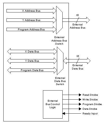
Figure 4‑1:
Example DSP processor
external memory interface. The processor has
three sets of on-chip memory buses, but only one set of off-chip memory buses.
The on-chip buses are multiplexed such that any one of the on-chip bus sets can
be
connected to the off-chip bus set.
Some DSP processors do provide multiple off-chip memory ports. The Analog Devices ADSP-21020 provides an external program memory port (24-bit address, 48-bit data) and an external data memory port (32-bit address, 32-bit data). The Texas Instruments TMS320C30 provides one 24-bit address, 32-bit data external memory port, and one 13-bit address, 32-bit data external memory port, while the TMS320C40 has two identical 31-bit addresses, 32-bit data external memory ports. Similarly, the Motorola DSP96002 provides two identical 32-bit address and data bus sets. The cost of these devices is correspondingly higher than that of comparable processors with only one external memory port.
DSP processor external memory interfaces vary quite a bit in flexibility and sophistication. Some are relatively simple and straightforward, with only a handful of control pins. Others are much more complex, providing the flexibility to interface with a wider range of external memory devices and buses without special interfacing hardware. Some of the features distinguishing external memory interfaces are the flexibility and granularity of programmable wait states, the inclusion of a wait pin to signal the availability of external memory, bus request and bus grant pins (discussed below), and support for page-mode DRAM (discussed below).
High-performance applications must often use fast static RAM devices for off-chip memory. In such situations, it is important for system hardware designers to scrutinize the timing specifications for DSP processors' external memory ports. Because timing specifications can vary significantly among processors, it is common to find two processors that have the same instruction cycle time but have very different timing specifications for off-chip memory. These differences can have a serious impact on system cost, because faster memories are significantly more expensive than slower memories. Hardware design flexibility is also affected, since more stringent timing specifications may constrain the hardware designer in terms of how the interface circuitry is designed and physically laid out.
4.4.1 Manual Caching
Whether or not a processor contains a cache, it is often possible for software developers to improve performance by explicitly copying sections of program code from slower or more congested (in terms of accesses) memory to faster or less congested memory. For example, if a section of often-used program code is stored in a slow, off-chip ROM, then it may make sense to copy that code to faster on-chip RAM, either at system start-up or when that particular program section is needed.
4.5 Multiprocessor Support in External Memory Interfaces
Interfaces DSP processors intended for use in multiprocessor systems often provide special features in their external memory interfaces to simplify the design and enhance the performance of such systems. The first and most obvious of these features is the provision of two external memory ports, mentioned above. The availability of two external memory ports means that one port can be connected to a local, private memory, while the other is connected to a memory shared with other processors. For example, the Motorola DSP96002 includes two external memory ports expressly for use in such multiprocessor configurations.
When a multiprocessor system includes two or more processors that share a single external memory bus, a mechanism must be provided for the processors to negotiate control of the bus (bus arbitration) and to prevent the processors that do not have control of the bus from trying to assert values onto the bus. Several DSP processors provide features to facilitate this kind of arrangement, though there are significant differences in the sophistication and flexibility of the features provided. In some cases, a shared bus multiprocessor can be created simply by connecting together the appropriate pins of the processors without the need for any special software or hardware to manage bus arbitration. In other cases, extra software on one or more of the DSP processors and/or external bus arbitration hardware may be required.
An example of basic support for shared bus systems is provided by the Motorola DSP5600x. Two of the DSP processor's pins can be configured to act as bus request and bus grant signals. When an external bus arbitrator (either another processor or dedicated hardware) wants a particular DSP processor to relinquish the shared bus, it asserts that processor's bus request input. The processor then completes any external memory access in progress and relinquishes the bus, acknowledging with the bus grant signal that it has done so. The DSP processor can continue to execute its program as long as no access to the shared bus is required. If an access to the shared bus is required, the processor waits until the bus request signal has been de-asserted, indicating that it can again use the shared bus.
The Texas Instruments TMS320C5x provides several features that support multiprocessing. In addition to providing the equivalent of bus request and bus grant signals (called HOLD and HOLDA on the TMS320C5x), the processor also allows an external device to access its on-chip memory. To accomplish this, the external device first asserts the TMS320C5x's HOLD input. When the processor responds by asserting HOLDA, the external device asserts BR, indicating that it wishes to access the TMS320C5x's on-chip memory. The TMS320C5x responds by asserting IAQ. The external device can then read and write the TMS320C5x's on-chip memory by driving TMS320C5x's address, data, and read/write lines. When finished, the external device deasserts HOLD and BR. This allows the creation of multiprocessor systems that do not require shared memory for interprocessor communications.
A processor feature that simplifies the use of shared variables in shared memory is bus locking, which allows a processor to read the value of a variable from memory, modify it, and write the new value back to memory, while ensuring that this sequence of operations is not interrupted by another processor attempting to update the variable's value. This is sometimes referred to as an atomic test-and-set operation. The Texas Instruments TMS320C3x and TMS320C4x processors provide special instructions and hardware support for bus locking; Texas Instruments refers to these operations as "interlocked operations."
The Analog Devices ADSP-2106x offers a sophisticated shared bus interface. The processor provides on-chip bus arbitration logic that allows direct interconnection of up to six ADSP-2106x devices with no special software or external hardware required for bus arbitration. In addition, the processor allows one DSP processor in a shared-bus configuration to access another processor's on-chip memory, much like on the Texas Instruments TMS320C5x family. This means that inter-processor data moves will not necessarily have to transit through an external shared memory.
In addition to special external memory interface features, the Analog Devices ADSP-2106x and the Texas Instruments TMS320C4x families provide special communications ports to facilitate connections within multiprocessor systems.
4.5.1 Dynamic Memory
All of the writable memory found on DSP processors and most of the memory found in systems based on DSP processors is static memory, also called SRAM (for static random-access memory; a better name would have been static read and write memory). Static memory is simpler to use and faster than dynamic memory (DRAM), but it also requires more silicon area and is more costly for a given number of bits of memory. The key operational attribute distinguishing static from dynamic memories is that static memories retain their data as long as power is available. Dynamic memories must be refreshed periodically; that is, a special sequence of signals must be applied to reinforce the stored data, or it eventually (typically in a few tens of milliseconds) is lost. In addition, interfacing to static memories is usually simpler than interfacing to dynamic memories; the use of dynamic memories usually requires a separate, external DRAM controller to generate the necessary control signals.
Because of the increasing proliferation of DSP processors into low-cost, high-volume products like answering machines and personal computer add-in cards, there has been increased interest in using dynamic memory in DSP systems. DRAM can also be attractive for systems that require large quantities of memory, such as large-scale multiprocessor systems.
One way to get faster, static RAM-like performance from slower, dynamic RAM is the use of paged or static column DRAM. These are special types of DRAM chips that allow faster than normal access when a group of memory accesses occur within the same region (or page) of memory. Some DSP processors, including the Motorola DSP96002, the Analog Devices ADSP-210xx, and the Texas Instruments TMS320C3x and TMS320C4x provide memory page boundary detection capabilities. These capabilities generally consist of a set of programmable registers, which the programmer uses to specify the locations of page boundaries in external memory, and circuitry to detect when external memory accesses cross page boundaries. In most cases, when the processor detects that a memory access has crossed a page boundary, it asserts a special output pin. It is then up to the external DRAM controller to use a processor input pin to signal back to the processor that it must delay its access by inserting wait states while the controller readies the DRAM for access to a new page.
As mentioned above, the use of DRAM as external memory for a DSP processor usually requires the use of an external DRAM controller chip. This additional chip may increase the manufacturing cost of the design, which partly defeats the reason for using DRAM in the first place. To address this problem, some DSP processors now incorporate a DRAM controller on-chip. The Motorola DSP56004 and DSP56007, for example, provide on-chip DRAM interfaces that include support for page-mode DRAM.
4.5.2 Direct Memory Access
Direct memory access (DMA) is a technique whereby data can be transferred to or from the processor's memory without the involvement of the processor itself. DMA is typically used to provide improved performance for input/output devices. Rather than have the processor read data from an I/O device and copy the data into memory or vice versa, a separate DMA controller can handle such transfers more efficiently. This DMA controller may be a peripheral on the DSP chip itself or it may be implemented using external hardware.
Any processor that has the simple bus request/bus grant mechanism described above can be used with an external DMA controller that accesses external memory. Typically the processor loads the DMA controller with control information including the starting memory address for the transfer, the number of data words to be transferred, the direction of the transfer, and the source or destination peripheral. The DMA controller uses the bus request pin to notify the DSP processor that it is ready to make a transfer to or from external memory. The DSP processor completes its current instruction, relinquishes control of external memory, and signals the DMA controller via the bus grant pin that the DMA transfer can proceed. The DMA controller then transfers the specified number of data words and optionally signals completion to the processor through an interrupt.
Some more sophisticated DSP processors include a DMA controller on-chip that can access internal and external memory. These DMA controllers vary in their performance and flexibility. In some cases, the processor's available memory bandwidth may be large enough to allow DMA transfers to occur in parallel with normal program instruction and data transfers without any impact on performance. For example, the Texas Instruments TMS320C4x contains a DMA controller that, combined with the TMS320C4x's on-chip memory and on-chip DMA address and data buses, can complete one memory access per instruction cycle independent of the processor. The Motorola DSP96002, the Texas Instruments TMS320C3x family, and the Analog Devices ADSP-2106x family all include on-chip DMA controllers with similar capabilities.
Some DMA controllers can manage multiple DMA transfers in parallel. Such a DMA controller is said to have multiple channels, each of which can manage one transfer, and each of which has its own set of control registers. The TMS320C4x DMA controller supports six channels, the Analog Devices ADSP-2106x supports ten channels, and the Motorola DSP96002 can handle two channels. Each channel can be used for memory-memory or memory-peripheral transfers.
In contrast, the AT&T DSP3210 includes a more limited, two-channel DMA controller that can only be used for transfers to and from the processor's internal serial port. Since the DSP3210 does not have extra memory bandwidth, the currently executing instruction is forced to wait one cycle when the DMA controller accesses memory. This arrangement (where the processor is suspended during DMA bus accesses) is called cycle stealing. The Analog Devices ADSP-21xx provides a similar capability through a mechanism that Analog Devices calls auto buffering.
5 Review of DSP Processors
Although there are many DSP processors, they are mostly designed with the same few basic operations in mind: so they share the same set of basic characteristics. We can learn a lot by considering how each processor differs from its competitors, and so gaining an understanding of how to evaluate one processor against others for particular applications.
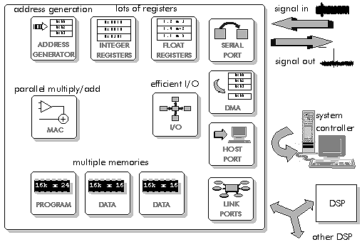
Figure 5‑1: Block diagram of a generalized DSP processor.
5.1 DSP32C - ADSP21060
Figure 5‑1 shows a generalized DSP processor, with the basic features that are common. These features can be seen in Figure 5‑2 for one of the earliest DSP processors - the Lucent DSP32C:

Figure 5‑2: The block diagram of the DSP32C.
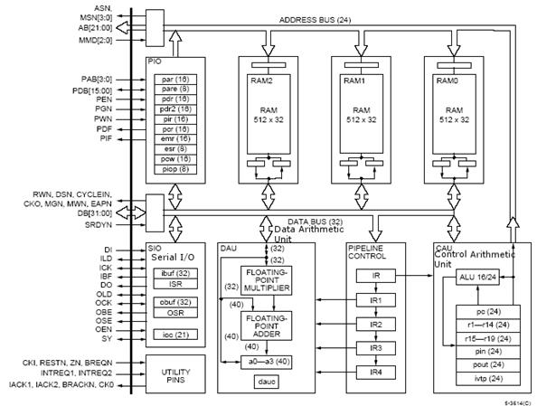
Figure 5‑3: Block diagram of the DSP32C with external memory interface.
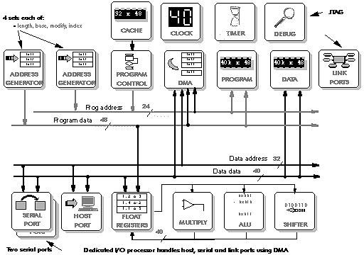
Figure 5‑4: Block diagram of the ADSP21060 processor.

Figure 5‑5: Detailed functional diagram of ADSP21060.
The Lucent DSP32C has four memory areas (three internal plus one external), and uses a modified von Neumann architecture to achieve four memory accesses per instruction cycle - the von Neumann architecture is shown by the presence of only a single memory bus (Figure 5‑3). It has four floating point registers: the address generation registers also double as general purpose fixed point registers. The Lucent DSP32C has a host port: showing that this chip is designed to be integrated into systems with another system controller - in this case, a microcontroller or PC (ISA) bus.
Looking at one of the more recent DSP processors - the Analog Devices ADSP21060 - shows how similar are the basic architectures (Figure 5‑4).
The ADSP21060 has Harvard architecture - shown by the two memory buses (Figure 5‑5). This is extended by a cache, making it a Super Harvard Architecture (SHARC). Note, however, that the Harvard architecture is not fully brought off chip - there is a special bus switch arrangement which is not shown on the diagram. The 21060 has two serial ports in place of the Lucent DSP32C's one. Its host port implements a PCI bus rather than the older ISA bus. Apart from this, the 21060 introduces four features not found on the Lucent DSP32C:
- There are two sets of address generation registers. DSP processors commonly have to react to interrupts quickly - the two sets of address generation registers allow for swapping between register sets when an interrupt occurs, instead of having to save and restore the complete set of registers.
- There are six link ports, used to connect with up to six other 21060 processors: showing that this processor is intended for use in multiprocessor designs.
- There is a timer - useful to implement DSP multitasking operating system features using time slicing.
- There is a debug port - allowing direct non-intrusive debugging of the processor internals.
5.2 DSP16A
A simple processor design like the Lucent DSP32C shows the basic features of a DSP processor: multiple on-chip memories, external memory bus, hardware add and multiply in parallel, lots of registers, serial interface, and host interface.
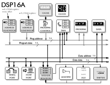
Figure 5‑6: Block diagram of the DSP16C.
The DSP32C is unusual in having a true von Neumann architecture: rather than use multiple buses to allow multiple memory accesses, it handles up to four sequential memory accesses per cycle. The DMA controller handles serial I/O, independently in and out, using cycle stealing which does not disturb the DSP execution thread.
The simple DSP32C design uses the address registers to hold integer data (Figure 5‑3): and there is no hardware integer multiplier: astonishingly, integers have to be converted to floating point format, then back again, for multiplication. We can excuse this lack of fast integer support by recalling that this was one of the first DSP processors, and it was designed specifically for floating point, not fixed point, and operation: the address registers are for address calculations, with integer operations being only a bonus.
For a fixed point DSP, the address generation needs to be separated from the integer data registers. This may also be efficient for a floating point DSP if integer calculations are needed very often. Lucent's more modern fixed point DSP16A processor shows the separation of fixed point from address registers (Figure 5‑6). The DSP16A also shows a more conventional use of multiple internal buses (Harvard plus cache) to access two memory operands (plus an instruction). A further arithmetic unit (shifter) has been added.
5.3 ADSP2181 - ADSP21060
DSP often involves a need to switch rapidly between one task and another: for example, on the occurrence of an interrupt. This would usually require all registers currently in use to be saved, and then restored after servicing the interrupt. The DSP16A and the Analogue Devices ADSP2181 use two sets of address generation registers:
The two sets of address generation registers can be swapped as a fast alternative to saving and restoring registers when switching between tasks. The ADSP2181 also has a timer: useful for implementing 'time sliced' task switching, such as in a real time operating system - and another indication that this processor was designed with task switching in mind (Figure 5‑7, Figure 5‑8).
It is interesting to see how far a manufacturer carries the same basic processor model into their different designs. Texas Instruments, Analog Devices and Motorola all started with fixed point devices, and have carried forward those designs into their floating point processors. AT&T (now Lucent) started with floating point, and then brought out fixed point devices later.
The Analog Devices ADSP21060 looks like a floating point version of the integer ADSP2181 (Figure 5‑5). The 21060 also has six high speed link ports which allow it to connect with up to six other processors of the same type. One way to support multiprocessing is to have many fast inter-processor communications ports: another is to have shared memory. The ADSP21060 supports both methods. Shared memory is supported in a very clever way: each processor can directly access a small area of the internal memory of up to four other processors. As with the ADSP2181, the 21060 has lots of internal memory: the idea being, that most applications can work without added external memory: note, though, that the full Harvard architecture is not brought off chip, which means they really need the on-chip memory to be big enough for most applications.
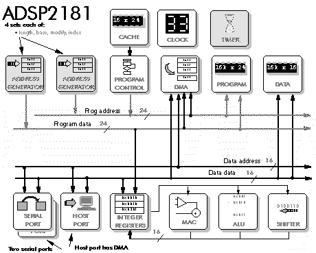
Figure 5‑7: Block diagram of the ADSP2181.

Figure 5‑8: Functional Block diagram of the ADSP2181.
5.4 DSP56002 – DSP56156 – DSP96002
The problem of fixed point processors is quantization error, caused by the limited fixed point precision. Motorola reduce this problem in the DSP56002 by using a 24 bit integer word length (Figure 5‑9, Figure 5‑10). They also use three internal buses - one for program, two for data (two operands). This is an extension of the standard Harvard architecture which goes beyond the usual trick of simply adding a cache, to allow access to two operands and the instruction at the same time.
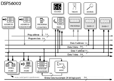
Figure 5‑9: Block diagram of the DSP56002.
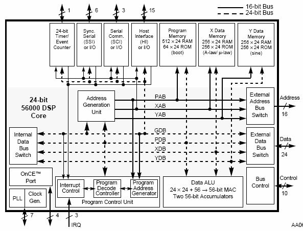
Figure 5‑10: Detailed functional block diagram of the DSP56002.
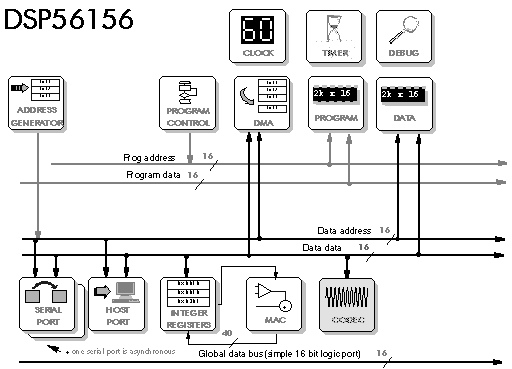
Figure 5‑11: Block diagram of the DSP56156.
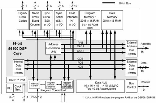
Figure 5‑12: Detailed functional block diagram of the DSP56156.
The problem of 24 bit fixed point is the expense of DSP56002, which probably explains why Motorola later produced the cheap, 16 bit DSP56156 - although this looks like a 16 bit variant of the DSP56002 (Figure 5‑11, Figure 5‑12). And of course there has to be a floating point variant, the DSP96002 looks like a floating point version of the DSP56002 (Figure 5‑13, Figure 5‑14). The DSP96002 supports multiprocessing with an additional global bus which can connect to other DSP96002 processors, it also has a new DMA controller with its own bus.
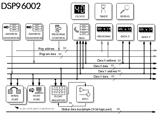
Figure 5‑13: Block diagram of the DSP96002.
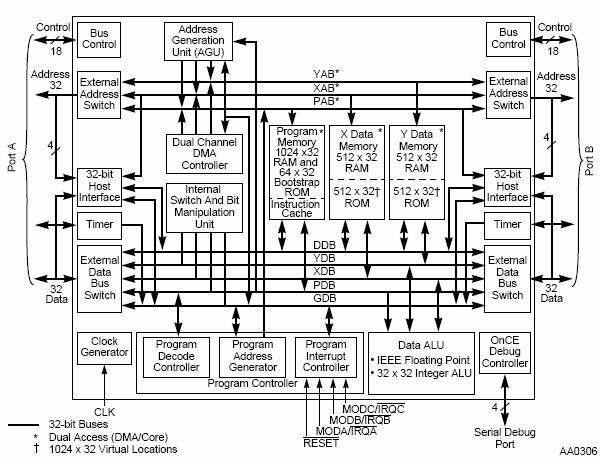
Figure 5‑14: Detailed functional block diagram of the DSP96002.
5.5 TMS320C25 - TMS320C50 - TMS320C30 - TMS320C40
The Texas TMS320C25 is quite an early design (Figure 5‑15, Figure 5‑16). It does not have a parallel multiply/add: the multiply is done in one cycle, the add in the next and the DSP has to address the data for both operations. It has a modified Harvard bus with only one data bus, which sometimes restricts data memory accesses to one per cycle, but it does have a special 'repeat' instruction to repeat an instruction without writing code loops
The Texas TMS320C50 is the C25 brought up to date (Figure 5‑17): the multiply/add can now achieve single cycle execution if it is done in a hardware repeat loop. It also uses shadow registers as a fast way to preserve registers when context switching. It has automatic saturation or rounding (but it needs it, since the accumulator has no guard bits to prevent overflow), and it has parallel bit manipulation which is useful in control applications.
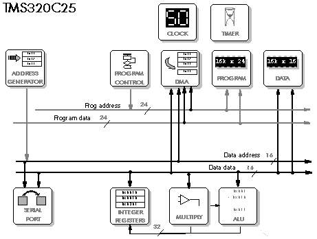
Figure 5‑15: Block diagram of TMS320C25.
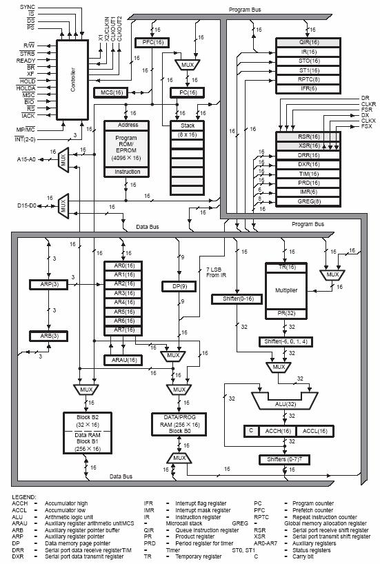
Figure 5‑16: Functional block diagram of TMS320C25.
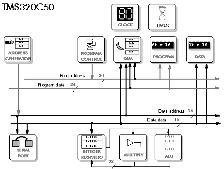
Figure 5‑17: Block diagram of the TMS320C50.
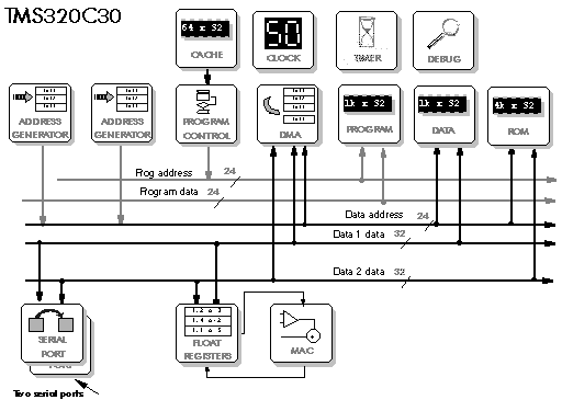
Figure 5‑18: Block diagram of the TMS320C30.
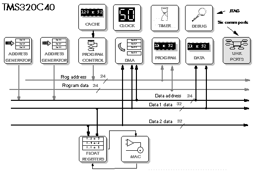
Figure 5‑19: Block diagram of the TMS320C40.
The Texas TMS320C30 carries on some of the features of the integer C25, but introduces some new ideas (Figure 5‑18). It has a von Neuman architecture with multiple memory accesses in one cycle, but there are still separate internal buses which are multiplexed onto the CPU. It also has a dedicated DMA controller.
The Texas TMS320C40 is similar to the C30, but with high speed communications ports for multiprocessing (Figure 5‑19). It has six high speed parallel comm ports which connect with other C40 processors: these are 8 bits wide, but carry 32 bit data in four successive cycles.
5.6 TMS320C60
The Texas TMS320C60 is radically different from other DSP processors, in using a Very Long Instruction Word (VLIW) format. It issues a 256 bit instruction, containing up to 8 separate 'mini instructions' to each of 8 functional units.
Because of the radically different concept, it an be hard to compare this processor with other, more traditional, DSP processors. But despite this, the 'C60 can still be viewed in a similar way to other DSP processors, which makes apparent the fact that it basically has two data paths each capable of a multiply/accumulate.
Note that Figure 5‑20 is very different from the way Texas Instruments draw it. This is for several reasons:
- Texas Instruments tend to draw their processors as a set of subsystems, each with a separate block diagram
- my diagram does not show some of the more esoteric features such as the bus switching arrangement to address the multiple external memory accesses that are required to load the eight 'mini-instructions'
An important point is raised by the placing of the address generation unit on the diagram. Texas Instruments draw the C60 block diagram as having four arithmetic units in each data path - whereas my diagram shows only three. The fourth unit is in fact the address generation calculation. Following my practice for all other DSP processors, I show address generation as separate from the arithmetic units - address calculation being assumed by the presence of address registers as is the case in all DSP processors. The C60 can in fact choose to use the address generation unit for general purpose calculations if it is not calculating addresses - this is similar, for example, to the Lucent DSP32C: so Texas Instruments' approach is also valid - but for most classic DSP operations address generation would be required and so the unit would not be available for general purpose use.
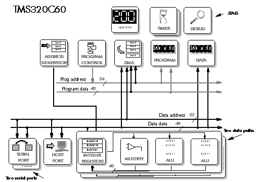
Figure 5‑20: Block diagram of the TMS320C60.
There is an interesting side effect of this. Texas Instruments rate the C60 as a 1600 MIPS device - on the basis that it runs at 200 MHz, and has two data paths each with four execution units: 200 MHz x 2 x 4=1600 MIPS. But from my diagram, treating the address generation separately, we see only three execution units per data path: 200 MHz x 2 x 3=1200 MIPS. The latter figure is that actually achieved in quoted benchmarks for an FIR filter, and reflects the device's ability to perform arithmetic.
This illustrates a problem in evaluating DSP processors. It is very hard to compare like with like - not least, because all manufacturers present their designs in such a way that they show their best performance. The lesson to draw is that one cannot rely on MIPS, MOPS or Mflops ratings but must carefully try to understand the features of each candidate processor and how they differ from each other - then make a choice based on the best match to the particular application. It is very important to note that a DSP processor's specialized design means it will achieve any quoted MIPS, MOPS or MFlops rating only if programmed to take advantage of all the parallel features it offers.
6 Choosing the Right DSP Processor
The right DSP processor for a job depends heavily on the application. One processor may perform well for some applications, but be a poor choice for others. With this in mind, one can consider a number of features that vary from one DSP to another in selecting a processor. These features are discussed below.
6.1 Arithmetic Format
One of the most fundamental characteristics of a programmable digital signal processor is the type of native arithmetic used in the processor. Most DSPs use fixed point arithmetic, while other processors using floating-point arithmetic. Floating-point arithmetic is a more flexible and general mechanism than fixed-point. With floating-point, system designers have access to wider dynamic range (the ratio between the largest and smallest numbers that can be represented). As a result, floating-point DSP processors are generally easier to program than their fixed point cousins, but usually are also more expensive and have higher power consumption. The increased cost and power consumption result from the more complex circuitry required within the floating-point processor, which implies a larger silicon die. The ease-of-use advantage of floating-point processors is due to the fact that in many cases the programmer doesn’t have to be concerned about dynamic range and precision. In contrast, on a fixed-point processor, programmers often must carefully scale signals at various stages of their programs to ensure adequate numeric precision with the limited dynamic range of the fixed-point processor. Most high-volume, embedded applications use fixed point processors because the priority is on low cost and, often, low power. Programmers and algorithm designers determine the dynamic range and precision needs of their application, either analytically or through simulation, and then add scaling operations into the code if necessary.
For applications that have extremely demanding dynamic range and precision requirements, or where ease of development is more important than unit cost, floating-point processors have the advantage. It’s possible to perform general-purpose floating point arithmetic on a fixed-point processor by using software routines that emulate the behavior of a floating point device. However, such software routines are usually very expensive in terms of processor cycles. Consequently, general-purpose floating-point emulation is seldom used. A more efficient technique to boost the numeric range of fixed-point processors is block floating point, wherein a group of numbers with different mantissas but a single, common exponent are processed as a block of data. Block floating-point is usually handled in software, although some processors have hardware features to assist in its implementation.
6.2 Data Width
All common floating-point DSPs use a 32-bit data word. For fixed-point DSPs, the most common data word size is 16 bits. Motorola’s DSP563xx family uses a 24-bit data word, however, while Zoran’s ZR3800x family uses a 20-bit data word. The size of the data word has a major impact on cost, because it strongly influences the size of the chip and the number of package pins required, as well as the size of external memory devices connected to the DSP. Therefore, designers try to use the chip with the smallest word size that their application can tolerate.
As with the choice between fixed and floating point chips, there is often a trade-off between word size and development complexity. For example, with a 16-bit fixed-point processor, a programmer can perform double-precision 32-bit arithmetic operations by stringing together an appropriate combination of instructions. (Of course, double-precision arithmetic is much slower than single-precision arithmetic.) If the bulk of an application can be handled with single-precision arithmetic, but the application needs more precision for a small section of the code, the selective use of double-precision arithmetic may make sense. If most of the application requires more precision, a processor with a larger data word size is likely to be a better choice.
Note that while most DSP processors use an instruction word size equal to their data word size, not all does. The Analog Devices ADSP-21xx family, for example, uses a 16-bit data word and a 24-bit instruction word.
6.3 Speed
A key measure of the suitability of a processor for a particular application is its execution speed. There are a number of ways to measure a processor’s speed. Perhaps the most fundamental is the processor’s instruction cycle time: the amount of time required to execute the fastest instruction on the processor. The reciprocal of the instruction cycle time divided by one million and multiplied by the number of instructions executed per cycle is the processor’s peak instruction execution rate in millions of instructions per second, or MIPS.
A problem with comparing instruction execution times is that the amount of work accomplished by a single instruction varies widely from one processor to another. Some of the newest DSP processors use VLIW (very long instruction word) architectures, in which multiple instructions are issued and executed per cycle. These processors typically use very simple instructions that perform much less work than the instructions typical of conventional DSP processors. Hence, comparisons of MIPS ratings between VLIW processors and conventional DSP processors can be particularly misleading, because of fundamental differences in their instruction set styles.
Even when comparing conventional DSP processors, however, MIPS ratings can be deceptive. Although the differences in instruction sets are less dramatic than those seen between conventional DSP processors and VLIW processors, they are still sufficient to make MIPS comparisons inaccurate measures of processor performance. For example, some DSPs feature barrel shifters that allow multi-bit data shifting (used to scale data) in just one instruction, while other DSPs require the data to be shifted with repeated one-bit shift instructions. Similarly, some DSPs allow parallel data moves (the simultaneous loading of operands while executing an instruction) that are unrelated to the ALU instruction being executed, but other DSPs only support parallel moves that are related to the operands of an ALU instruction.
Some newer DSPs allow two MACs to be specified in a single instruction, which makes MIPS-based comparisons even more misleading. One solution to these problems is to decide on a basic operation (instead of an instruction) and use it as a yardstick when comparing processors. A common operation is the MAC operation. Unfortunately, MAC execution times provide little information to differentiate between processors: on many DSPs a MAC operation executes in a single instruction cycle, and on these DSPs the MAC time is equal to the processor’s instruction cycle time.
And, as mentioned above, some DSPs may be able to do considerably more in a single MAC instruction than others. Additionally, MAC times don’t reflect performance on other important types of operations, such as looping, that are present in virtually all applications. A more general approach is to define a set of standard benchmarks and compare their execution speeds on different DSPs. These benchmarks may be simple algorithm “kernel” functions (such as FIR or IIR filters), or they might be entire applications or portions of applications (such as speech coders). Implementing these benchmarks in a consistent fashion across various DSPs and analyzing the results can be difficult.
Two final notes of caution on processor speed: First, be careful when comparing processor speeds quoted in terms of “millions of operations per second” (MOPS) or “millions of floating-point operations per second” (MFLOPS) figures, because different processor vendors have different ideas of what constitutes an “operation.” For example, many floating-point processors are claimed to have a MFLOPS rating of twice their MIPS rating, because they are able to execute a floating-point multiply operation in parallel with a floating-point addition operation. Second, use caution when comparing processor clock rates. A DSP’s input clock may be the same frequency as the processor’s instruction rate, or it may be two to four times higher than the instruction rate, depending on the processor. Additionally, many DSP chips now feature clock doublers or phase-locked loops (PLLs) that allow the use of a lower-frequency external clock to generate the needed high-frequency clock onchip.
6.4 Memory Organization
The organization of a processor’s memory subsystem can have a large impact on its performance. As mentioned earlier, the MAC and other DSP operations are fundamental to many signal processing algorithms. Fast MAC execution requires fetching an instruction word and two data words from memory at an effective rate of once every instruction cycle. There are a variety of ways to achieve this, including multiported memories (to permit multiple memory accesses per instruction cycle), separate instruction and data memories (the “Harvard” architecture and its derivatives), and instruction caches (to allow instructions to be fetched from cache instead of from memory, thus freeing a memory access to be used to fetch data).
Another concern is the size of the supported memory, both on- and off-chip. Most fixed-point DSPs are aimed at the embedded systems market, where memory needs tend to be small. As a result, these processors typically have small-to-medium on-chip memories (between 4K and 64K words), and small external data buses. In addition, most fixed-point DSPs feature address buses of 16 bits or less, limiting the amount of easily-accessible external memory.
Some floating-point chips provide relatively little (or no) on-chip memory, but feature large external data buses. For example, the Texas Instruments TMS320C30 provides 6K words of on-chip memory, one 24-bit external address bus, and one 13-bit external address bus. In contrast, the Analog Devices ADSP-21060 provides 4 Mbits of memory on-chip that can be divided between program and data memory in a variety of ways. As with most DSP features, the best combination of memory organization, size, and number of external buses is heavily application-dependent.
6.5 Ease of Development
The degree to which ease of system development is a concern depends on the application. Engineers performing research or prototyping will probably require tools that make system development as simple as possible. That said, items to consider when choosing a DSP are software tools (assemblers, linkers, simulators, debuggers, compilers, code libraries, and real-time operating systems), hardware tools (development boards and emulators), and higher-level tools (such as block-diagram based code-generation environments). A fundamental question to ask when choosing a DSP is how the chip will be programmed. Typically, developers choose either assembly language, a high-level language—such as C or Ada—or a combination of both. Surprisingly, a large portion of DSP programming is still done in assembly language. Because DSP applications have voracious number-crunching requirements, programmers are often unable to use compilers, which often generate assembly code that executes slowly. Rather, programmers can be forced to hand-optimize assembly code to lower execution time and code size to acceptable levels. Users of high-level language compilers often find that the compilers work better for floating-point DSPs than for fixed-point DSPs, for several reasons. First, most high-level languages do not have native support for fractional arithmetic. Second, floating-point processors tend to feature more regular, less restrictive instruction sets than smaller, fixed-point processors, and are thus better compiler targets. Third, as mentioned, floating point processors typically support larger memory spaces than fixed-point processors, and are thus better able to accommodate compiler-generated code, which tends to be larger than hand crafted assembly code.
VLIW-based DSP processors, which typically use simple, orthogonal RISC-based instruction sets and have large register files, are somewhat better compiler targets than traditional DSP processors. However, even compilers for VLIW processors tend to generate code that is inefficient in comparison to hand-optimized assembly code. Hence, these processors, too, are often programmed in assembly language—at least to some degree. Whether the processor is programmed in a high-level language or in assembly language, debugging and hardware emulation tools deserve close attention since, sadly, a great deal of time may be spent with them. Almost all manufacturers provide instruction set simulators, which can be a tremendous help in debugging programs before hardware is ready. If a high-level language is used, it is important to evaluate the capabilities of the high-level language debugger: will it run with the simulator and/or the hardware emulator? Is it a separate program from the assembly-level debugger that requires the user to learn another user interface? Most DSP vendors provide hardware emulation tools for use with their processors. Modern processors usually feature on-chip debugging/emulation capabilities, often accessed through a serial interface that conforms to the IEEE 1149.1 JTAG standard for test access ports. This serial interface allows scan-based emulation—programmers can load breakpoints through the interface, and then scan the processor’s internal registers to view and change the contents after the processor reaches a breakpoint.
Scan-based emulation is especially useful because debugging may be accomplished without removing the processor from the target system. Other debugging methods, such as pod-based emulation, require replacing the processor with a special processor emulator pod. Off-the-shelf DSP system development boards are available from a variety of manufacturers, and can be an important resource. Development boards can allow software to run in real-time before the final hardware is ready, and can thus provide an important productivity boost. Additionally, some low-production-volume systems may use development boards in the final product.
6.6 Multiprocessor Support
Certain computationally intensive applications with high data rates (e.g., radar and sonar) often demand multiple DSP processors. In such cases, ease of processor interconnection (in terms of time to design interprocessor communications circuitry and the cost of linking processors) and interconnection performance (in terms of communications throughput, overhead, and latency) may be important factors. Some DSP families—notably the Analog Devices ADSP-2106x—provide special-purpose hardware to ease multiprocessor system design. ADSP-2106x processors feature bidirectional data and address buses coupled with six bidirectional bus request lines. These allow up to six processors to be connected together via a common external bus with elegant bus arbitration. Moreover, a unique feature of the ADSP-2106x processor connected in this way is that each processor can access the internal memory of any other ADSP-2106x on the shared bus. Six four-bit parallel communication ports round out the ADSP-2106x’s parallel processing features.
6.7 Power Consumption and Management
DSPs are increasingly being used in portable applications (such as cellular phones and portable audio players) where power consumption is a major concern. As a result, many processor vendors are reducing processor supply voltages and adding power management features to give programmers greater influence over processor power consumption. Power management features available on some DSPs include:
Reduced voltage operation: Many vendors offer low-voltage (3.3-, 2.5-, or 1.8-volt) versions of their DSP processors. These processors consume far less power than five-volt equivalents at the same clock rate.
Sleep or idle modes: Most DSPs feature modes that turn off the processor’s clock to all but certain sections of the processor, reducing power consumption. In some cases, any unmasked interrupt will bring the processor back from sleep mode, while in other cases, only a few designated external interrupt lines will wake the processor. Some processors provide multiple sleep modes with different power savings and wakeup latencies.
Programmable clock dividers: Some DSPs allow the processor’s clock frequency to be varied under software control to use the minimum clock speed required for a particular task.
Peripheral control: Some DSPs allow the programmer to disable peripherals that are not in use. Regardless of power management features, it is often difficult for design engineers to obtain meaningful power consumption figures for DSPs. This is because a DSP’s power consumption may vary by as much as a factor of three depending on the instructions it executes.
Unfortunately, most vendors publish only “typical” or “maximum” power consumption numbers, usually without specifying what constitutes a “typical” program. One exception is Texas Instruments, which provides application notes that detail power consumption vs. instruction type and processor configuration.
6.8 Cost
Obviously, processor cost is a major concern for products that are to be produced in volume. For such applications, designers try to use the lowest cost DSP that meets the requirements of the application, even though such devices may be considerably less flexible and more difficult to program than costlier processors. Among processor families, the least expensive family members tend to have significantly fewer features, less on-chip memory, and lower performance than the more expensive members.
A key factor in processor pricing is the dependence of price on device packaging. For example, plastic thin quad flat pack (PQFP and TQFP) packages can be significantly less expensive than pin grid array (PGA) packages. Finally, when considering prices, it is important to remember two things. First, processor prices are continually falling. Second, prices are strongly dependent on quantity, and prices for, say, a quantity 100,000 order may be significantly lower than for a quantity 1,000 order.
References
[1] S. W. Smith. (1997) The Scientist and Engineer's Guide to Digital Signal Processing. (2nd Edition), California Technical Publishing, SanDieago..
[2] J. Bier, P. Lapsley , and G. Blalock . (1996) Choosing a DSP Processor, Berkeley Design Technology, Inc. Publication.
[3] P. Lapsley, J. Bier, A. Shoham, and E. A. Lee. (1996) DSP Processor Fundamentals: Architectures and Features, IEEE Press.
[4] M. M. Mano. (1991) Digital Design, (2nd Edition), Prentice Hall International Inc.
[5] Y. Langsam, M. J. Augenstein, and A. M. Tenenbaum. (1996) Data Structures Using C and C++, (2nd Edition), Prentice Hall International Inc.
[6] N. R. Scott. (1999) Analog and Digital Computer Technology, (International Student Edition), McGraw Hill Book Company Inc.
[7] Y. Chu. (2001) Digital Design Fundamentals, McGraw Hill Book Company Inc.
[8] Hitachi Microcomputer Data Book 4-Bit Single Chip, (1984), Hitachi Ltd. Press London.
[9] Hitachi Microcomputer Data Book: 8-/16-Bit Microprocessor, (1986), Hitachi Ltd. Press. London, vol. 12-83
[10] Intel Data Catalog. (1977). Intel Corporation Press, Belgium.
[11] David Goldberg. (1991) What Every Computer Scientist Should Know About Floating-Point Arithmetic, ACM Computing Surveys, Vol. 23, No. 1, March 1991, pp. 5-48
[12] Lucent DSP32C Digital Signal Processor. Data sheet, Lucent Technologies Inc., November 1996
[13] Analog Devices ADSP-2181 DSP Microcomputer. Data sheet, Analog Devices Inc., 1997, Rev. C
[14] Analog Devices ADSP-21060/ADSP-21060L ADSP-2106x SHARC DSP Microcomputer Family. Data sheet, Analog Devices Inc., 2000, Rev. D
[15] Motorola DSP56156 DSP56156ROM Product Information. Data sheet, Motorola Inc., 1994, DSP56156P/D
[16] Motorola DSP-56002/D Semiconductor Technical Data. Data sheet, Motorola Inc., 1996, Rev. 3
[17] Motorola DSP96002 Product Information. Data sheet, Motorola Inc., 1996, DSP96002P/D
[18] Texas Instruments TMS320 Second- Generation Digital Signal Processors. Data sheet, Texas Instruments Inc., November 1990, Ver. SPRS010B
[19] Texas Instruments TMS320C6713/TMS320C6713B Floating Point Digital Signal Processors. Data sheet, Texas Instruments Inc., December 2001 - Revised 2004
[20] ANSI/IEEE STD 754-1985 IEEE Standard for Binary Floating-Point Arithmetic, IEEE Standards Board, The Institute of Electrical and Electronics Engineers Inc., 1985
[21] ANSI/IEEE STD 854-1987 IEEE Standard for Radix-Independent Floating-Point Arithmetic, IEEE Standards Board, The Institute of Electrical and Electronics Engineers Inc.,1987
[22] H. Rongen. (2000). Introduction to Digital Signal Processors (DSPs). Julich, Germany.
[23] G. Blalock. (2004). The BDTIMark: A Measure of DSP Execution Speed. Berkeley Design Technology, Inc., White Paper.
[24] E. Tan, and W. Heinzelman. (2003). DSP Architectures: Past, Present and Future, Computer Architecture News, Vol. 31, No. 3, pp. 6-19.
[25] C. Hecker. (1996). Let’s Get to the (Floating) Point. Game Developer Magazine, Vol. Feb.March, pp. 19-24.
[26] A. Said. Introduction to Arithmetic Coding Theory and Practice, Hewlett-Packard Laboratories Report, HPL-2004-76, Palo Alto, CA, April 2004.
[27] B. Paillard. (2002) An Introduction to Digital Signal Processors, Génie électrique et informatique Report, Université de Sherbrooke, April 2004.
[28] M. F. Cowlishaw. (2003) Decimal Floating-Point: Algorism for Computers, Proceedings of the 16th IEEE Symposium on Computer Arithmetic (ARITH03), 1063-6889/03 IEEE.
[29] M. F. Cowlishaw. (2003) Decimal Arithmetic Encoding, IBM Laboratories UK Report, version 0.96.
APPENDIX A - IEEE Standard for Binary Floating Point Arithmetic

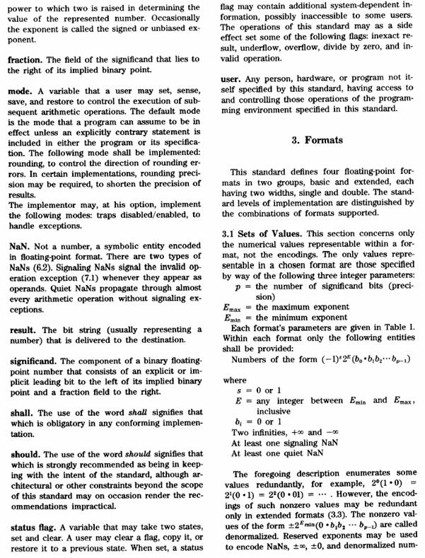
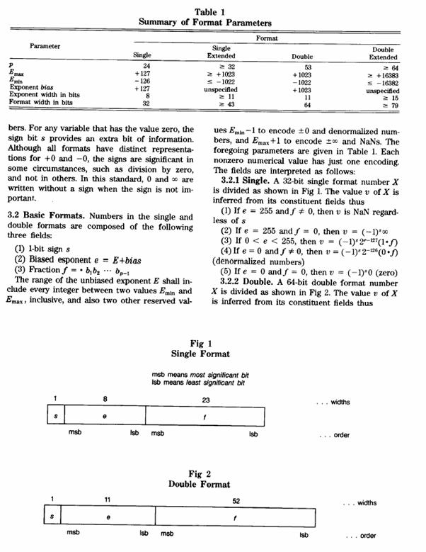

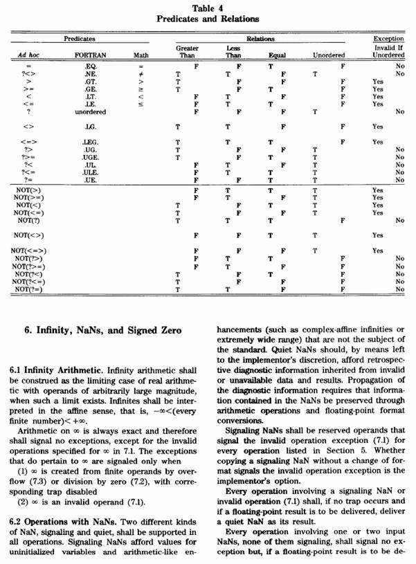
APPENDIX B - IEEE Standard for Radix-Independent Floating Point Arithmetic
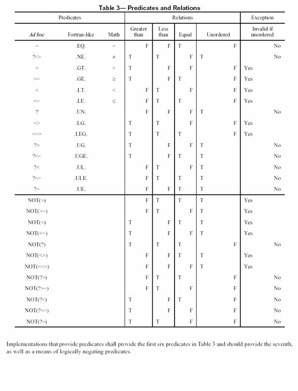
APPENDIX C – Calculation of Emax and bias
This section describes how Emax and Emin (the maximum and minimum exponents available in a format) and bias (the amount to be subtracted from the encoded exponent to form the exponent’s value) are calculated. Except for the calculation of Elimit, these calculations are general for any format where the coefficient and exponent are both integers.
1. Let p be the precision (total length of the coefficient) of a format, in digits.
2. Let Emax be the maximum positive exponent for a value in a format, as defined in IEEE 854. That is, the largest possible number is (10p-1) / (10(p–1)) × 10Emax
For example, if p=7 this is 9.999999 × 10Emax.
3. The exponent needed for the largest possible number is Emax–(p–1) (because, for example, the largest coefficient when p=7 is 9999999, and this only needs to be multiplied by
10Emax / 10(p–1) to give the largest possible number.
4. Emin=–Emax (as defined by IEEE 854 for base 10 numbers). That is, the smallest normal number is 10Emin. The exponent needed for this number is Emin (its coefficient will be 1).
5. The number of exponents, Enormals, used for the normal numbers is therefore 2 × Emax – p + 2. (The values –Emax through –1, 0, and 1 through Emax–(p–1).)
6. Let Etiny be the exponent of the smallest possible (tiniest, non-zero) subnormal number when expressed as a power of ten. This is Emin – (p–1). For example. if p=7 again, the smallest subnormal is 0.000001 × 10Emin, which is 10Etiny.
The number of exponents needed for the subnormal numbers, Esubnormals, is therefore Emin – Etiny, which is p – 1.
7. Let Erange be the number of exponents needed for both the normal and the subnormal numbers; that is, Enormals + Esubnormals. This is (2 × Emax + 1).
8. Place Etiny so its encoded exponent (the exponent with bias added) is 0 (the encoded exponent cannot be less than 0, and we want an all-zeros number to be valid – hence an encoded exponent of 0 must be valid).
9. Let Elimit be the maximum encoded exponent value available. For the formats in the specification, this is 3 × 2ecbits – 1, where ecbits is the length of the exponent continuation in bits (for example, Elimit is 191 for the 32-bit format).
10. Then, the number of exponent values available is Elimit + 1, which is 3 × 2ecbits.
11. Now, to maximize Emax, Erange = Elimit + 1
That is, 2 × Emax + 1 = 3 × 2ecbits.
12. Hence: Emax = (3 × 2ecbits – 1)/2 = Elimit/2
Note that the divisions by 2 must be truncating integer division.
13. If Elimit is odd (always the case in these encodings), one value of exponent would be unused. To make full use of the values available, Emin remains as the value just calculated, negated, and Emax is increased by one.7
Hence: Emin = –Elimit/2
and: Emax = Elimit/2 + 1 (where the divisions by 2 are truncating integer division).
14. And: bias = –Etiny = –Emin + p – 1
For example, let Elimit = 191 and p = 7 (the 32-bit format). Then:
Emax = 191/2 + 1 = 96
Emin = –95
Etiny = –101
bias = 101
The parameters and derived values for all three formats are as follows:
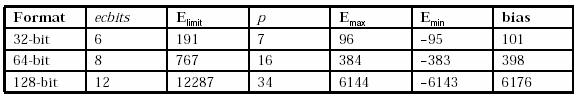
Note that it is also possible to consider the coefficients in these formats to have a decimal point after the first digit (instead of after the last digit). With this view, the bit patterns for the layouts are identical, but the bias would be decreased by p–1, resulting in the same value for a given number.